Looking back at Gamesphere
Before I write much about my Gameslab project, I think it’s worth looking back at my Gamesphere project from over four years ago. I still receive a handful of emails per month asking for schematics or help on building a new game console. Usually, these emails are desperate college seniors looking for an easy senior project. And, I’m afraid for the people that are legitimately looking for schematics to learn from, I didn’t make any. That’s part of why I want to look back on my previous project; I want to see what I can do better this time around, and also, what I did well the first time.
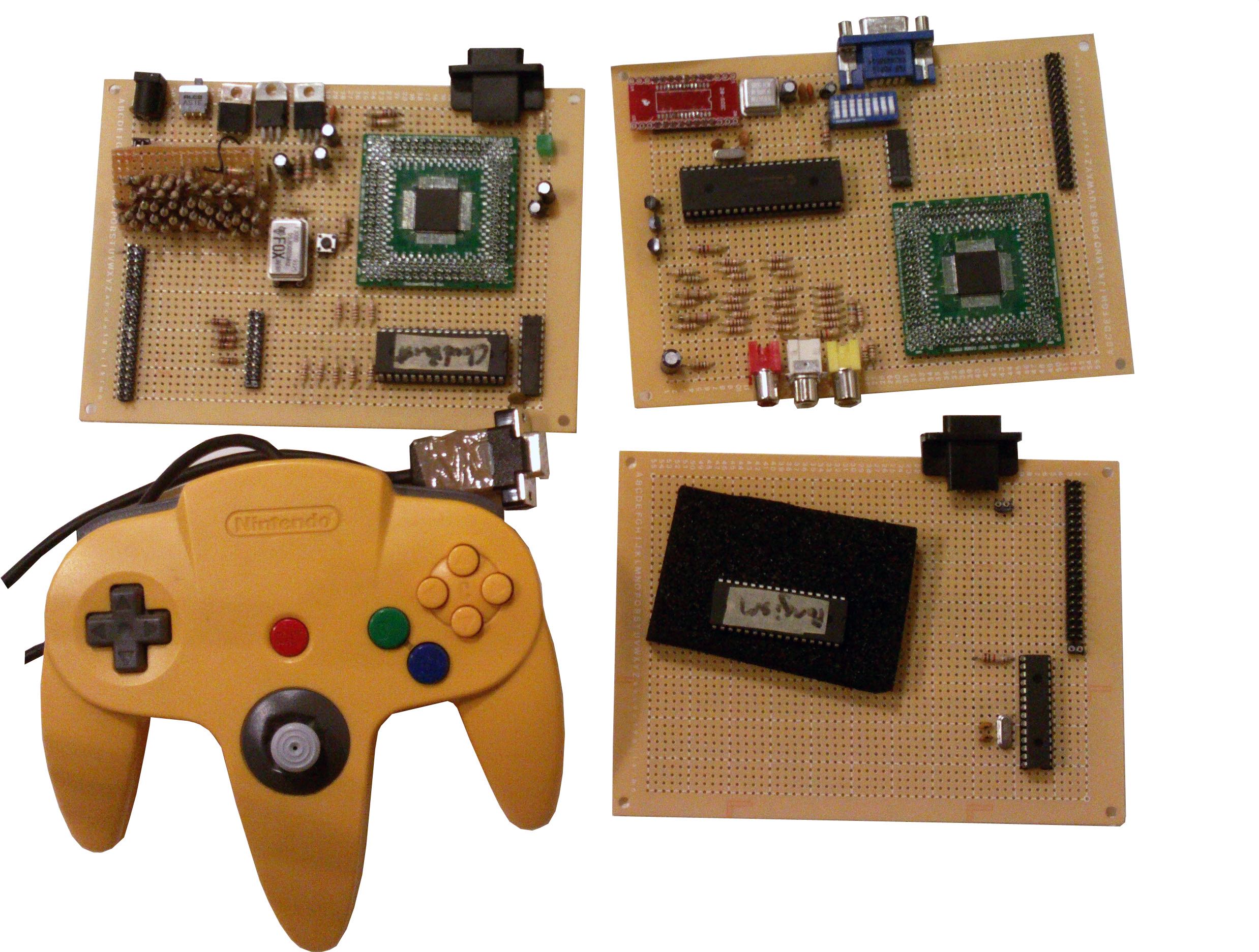 Top, from left to right: CPU board, video board; bottom: N64 controller, input board
I started building the first Gamesphere during my senior year of high school. I had already begun experimenting with PIC microcontrollers and other breadboard-able goodies before, but Gamesphere was my biggest project yet at the time.
I had already built several microcontroller-based game (-ish) projects using PIC microcontroller and some careful clock cycle counting. I don’t have any surviving photos, but I think the first one was a black-and-white pong game that generated NTSC video using a PIC18F452. Another project used a 128×128, 8-BPP cellphone screen, a few tactile switches, and a PIC18F4685. The cellphone screen used an SPI interface, so I had use dirty-rectangle techniques to achieve decent draw-rates. Having built several consoles, I really wanted to do something substantial. I found some incredible inspiration in André LaMothe’s book The Black Art of Video Game Console Design. Andre also used to maintain a website dedicated to the game consoles in the book, and a picture gallery of all the WIP consoles leading up to the XGameStation. I was inspired by the video in which Andre shows off several hundred lines of ARM assembly, assembles the project, burns it to an EPROM, and the boots the wire-wrapped ARM board–all to blink a LED. I wanted to do that.
I actually copied André’s choice of microcontroller, an Atmel AT91R40008. The AT91R40008 is a 32-bit ARM7/Thumb micro with a 16-bit external parallel bus. It was specified to run up to 75Mhz, but I’ve used my parts all the way to 100MHz. Atmel, at least back then, had a very generous free sample program. I signed up, said I was a student, and parts showed up two weeks later! In addition to samples, Atmel datasheets are incredibly good (AT91R40008 datasheet). Trust me, try using a Freescale, or even worse, a Cirrus datasheet.
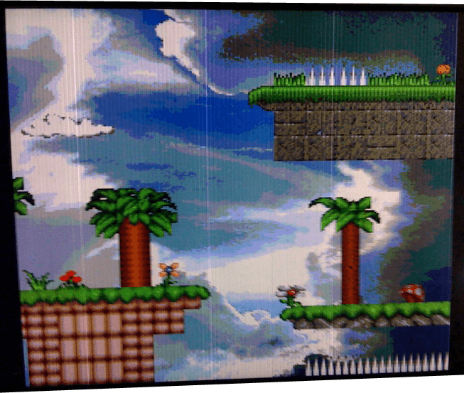 The vertical line artifacts are from SRAM bank cross-overs–one of the downsides of a direct DAC. Thank you Ari Feldman for SpriteLib
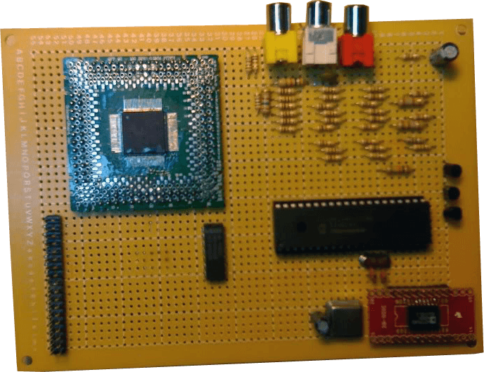
CPU Board
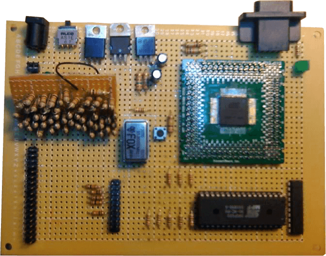 The big mass of resistors is my attempt at an R2R ladder audio DAC. It actually worked, but the tone was completely off. I never did figure out whether it was my sample-rate timer or the DAC itself.
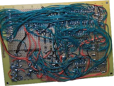 That is point-to-point soldering hell. Only when you’re in high school with gobs of free-time…
Now before you ask, no I don’t have schematics. That was actually one of my biggest mistakes: I simply added components and connections as I needed them. If you look at the point-to-point soldering hell on the bottom of the board, I feel like the lack of schematic is quite evident.
I started the CPU board with the power supply: just a standard barrel jack, a 7805 for 5V, a LD33V for 3.3V, and a LM317 set for 1.8V. Each power supply has its own status LED (hidden under the R2R DAC in the picture). There are also some miscellaneous electrolytic caps for filtering near the regulators. For the CPU reset switch, I used one of those ubiquitous through-hole tactile switches. For the CPU clock, I started with a FOX 55.8MHz 4-pin oscillator I had laying around from a grab-bag electronic component purchase. The main CPU is where things get interesting. Before this, I had little to zero knowledge of surface mount soldering. I definitely had zero knowledge to create a PCB layout. So, I ended up using a SchmartBoard TQFP100 to through-hole adapter board. SchmartBoards use an interesting method in which the trace for each SMT pin is actually a trench. Once the part is in place, you simply slide your fine soldering iron tip along the trench. Just don’t try it with one of those wood burner type irons. Once the TQFP100 package is in place, the only difficulty is keeping track of which pins on the package map to which pins on the adapter board. I ended using the continuity function on my multimeter a lot (just to double-check of course).
With the addition of a 20-pin JTAG header, it was actually possible to test the board. Most people use OpenOCD to talk JTAG with their ARM systems, but I could not make OpenOCD work at the time. I actually ended up using OCD Commander by Macraigor Systems. It’s a simple command-line interface for running JTAG commands–poking memory, blinking an LED manually, writing to the flash, etc. I created a simple ARM assembly program that would blink an attached LED indefinitely, assembled it with the GNU ARM toolchain, and poked it into memory using OCD Commander. That was an epic moment! After that, I added an SST 256KB NOR flash (I honestly have no memory of where I got that part). The SST flash part was very easy to implement though, as it did not require a separate programming voltage like some flash parts at the time. So, I could actually erase and reprogram the flash using the external memory interface alone.
Video Board
 Even though the audio DAC is on the CPU board, I put the audio RCA connectors on the video board, so they are next to the composite video connector.
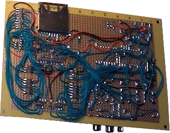 I never did get the SD card interface working. The AT91R40008 doesn’t have a SPI module, so I attempted to bit-bang the MMC protocol.
The Gamesphere’s video generation system uses a brute-force approach. In the pictures above, the TQFP100 package on another SchmartBoard is a CY7C009V dual-port asynchronous SRAM. With 128KB of dual-ported RAM, the CPU can write to one video buffer while the video board is drawing the other frame to the screen. The Gamesphere outputs 224×240 8 bits-per-pixel video to VGA. Each frame uses 53,760 bytes of RAM, under half of the dual-port RAM. To flip buffers, a GPIO pin on the CPU flips the highest-order bit on the dual-port RAM address lines. From the CPU’s side of the video interface, the screen appears as a bitmap. The CPU can write a pixel color at a specific address, flip the frame buffer, and the pixel will show up on the screen. If the CPU does not flip buffers during the vertical retrace, artifacts can show up on screen. So, the video board also provides a vertical synchronization interrupt to the host CPU.
On the other side of the dual-port RAM, a PIC18F4685 microcontroller counts addresses to the dual-port RAM according to the VGA timing specification. Using 640×480 VGA, each pixel of the Gamesphere’s framebuffer covers a 2×2 block of pixels on the screen. The PIC microcontroller runs an assembly program with clock-cycle-counted loops to increment the addresses to its side of the dual-port RAM. The data lines from the RAM are fed into R2R ladder DACs. Red has a 3-bit DAC, green has a 3-bit DAC, and blue has a 2-bit DAC. A few of NPN signal transistors are used to pull all the color lines to a blanking level during syncs pulses and blanking intervals. The final result still has some artifacts, I think due to either imperfections in my video timing code, or the dual-port RAM switching banks as I count addresses. I also attempted to generate composite video output using an AD725 RGB to NTSC/PAL converter IC. I could not reach the correct video timing, at least with the TV I had available for testing. Although, you can see a correct looking waveform in the oscilloscope below.
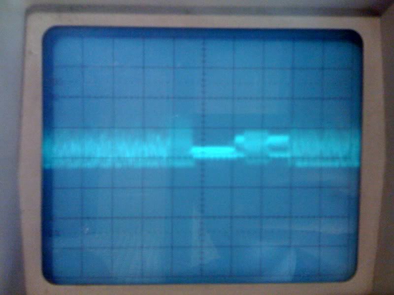 The display is triggered on the synchronization pulse in the center. NTSC video as a front-porch (low voltage level), a synch pulse (zero level), and a back porch (low level). Video data follows the back porch. Since NTSC is backward compatible, color data is actually modulated onto the existing B&W signal using phase shift modulation. To create a reference phase, the back-porch includes the ‘color burst’, which you can see right after the synch pulse in this image.
Input Board
I don’t have any better photos the the input board than the overview photo at the beginning of this post. It’s not a terribly exciting board anyway. It just has a DB9 connector that I used for connecting to an N64 controller. I actually modified the N64 controller itself to have a DB9 connector (much easier to find parts for). The board itself has on PIC micrcontroller (18F series again, free samples!) that talks to the main CPU over UART. The input controller runs a program that queries the N64 controller using the obscure and precisely timed protocol.
More photos
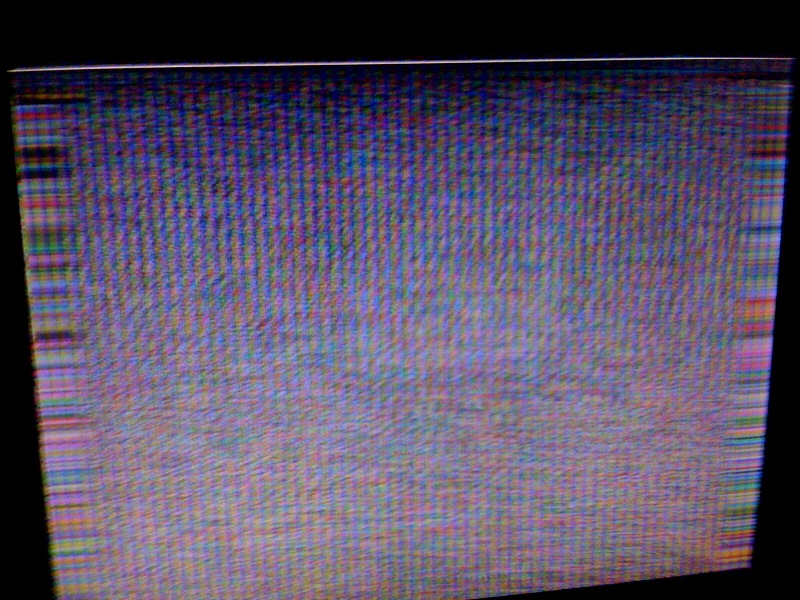 The video board did not work correctly at first, and it turned out to be very difficult to debug since different brands of monitors locked better/worse onto poorly timed VGA signals.
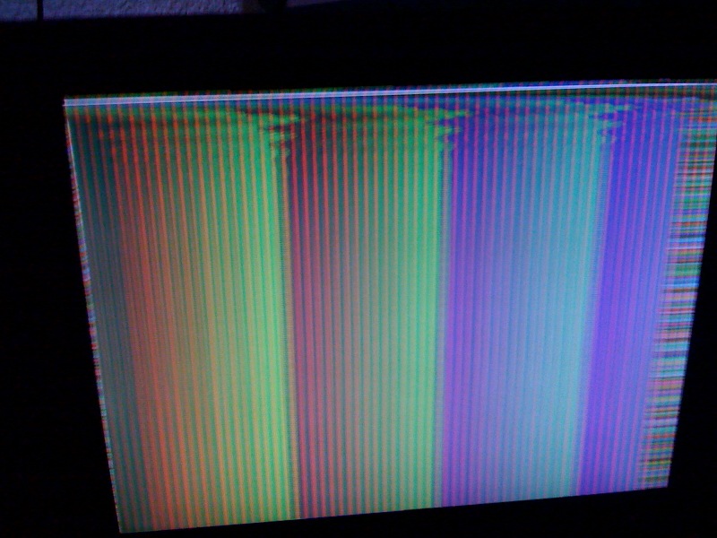 This photo shows some of the artifacts that a poorly timed signal can generate. You can visibly see the time the screen takes to lock onto the video signal.
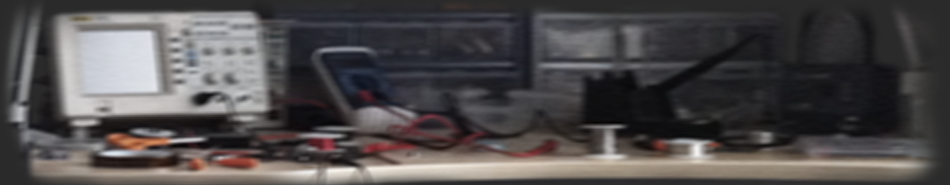
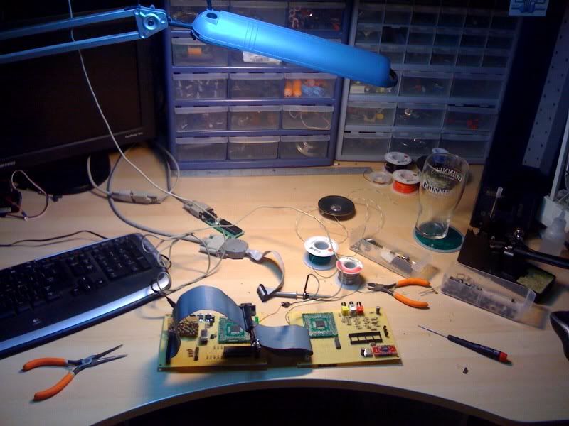 My workbench at the time; you can see the PIC and JTAG programmers in the middle of the desk.