
From eBay junk to JTAG on a gigantic FPGA board
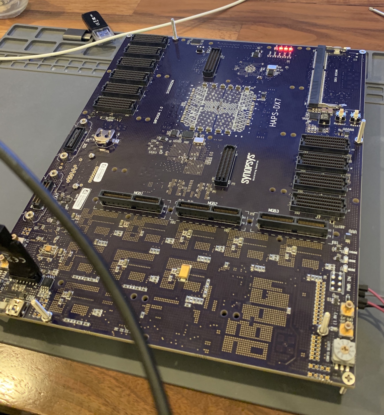
eBay is a magical place, somewhere in the middle of the vast AliExpress-Digikey spectrum… well, it is magical for those interested in giant FPGA parts anyway. In previous posts, I detailed the Gameslab, which is a handheld game console built around reballed Zynq (XC7Z035) parts off eBay, which turned out to be perfectly fine after fixing my own mistakes. So, I’m no stranger to the hopes and fears of buying used and unknown quality FPGA components off eBay. That said, thanks to @rombik_su on Twitter, I’m down an even deeper rabbit hole on a HAPS-DX7 board with a Xilinx Virtex-7 XC7VX980T (whopping 612 kLUTs), a smaller Kintex XC7K70T, and a relatively tiny Lattice LCMXO2-7000HC. I’ll try to document the journey in this post.
Here’s the tweet that kicked this fun adventure off. I probably need to filter out tweets that link to eBay in the future to prevent this from becoming a fully-developed habit.
Oh boy, Prolapsys HAPS DX-7 board for with XC7VX980T (980K cells) for $300 pic.twitter.com/PLsI8RbKMB
— Andrey Ø. (@rombik_su) December 2, 2020
An impulse-buy later, this board arrived on my desk.
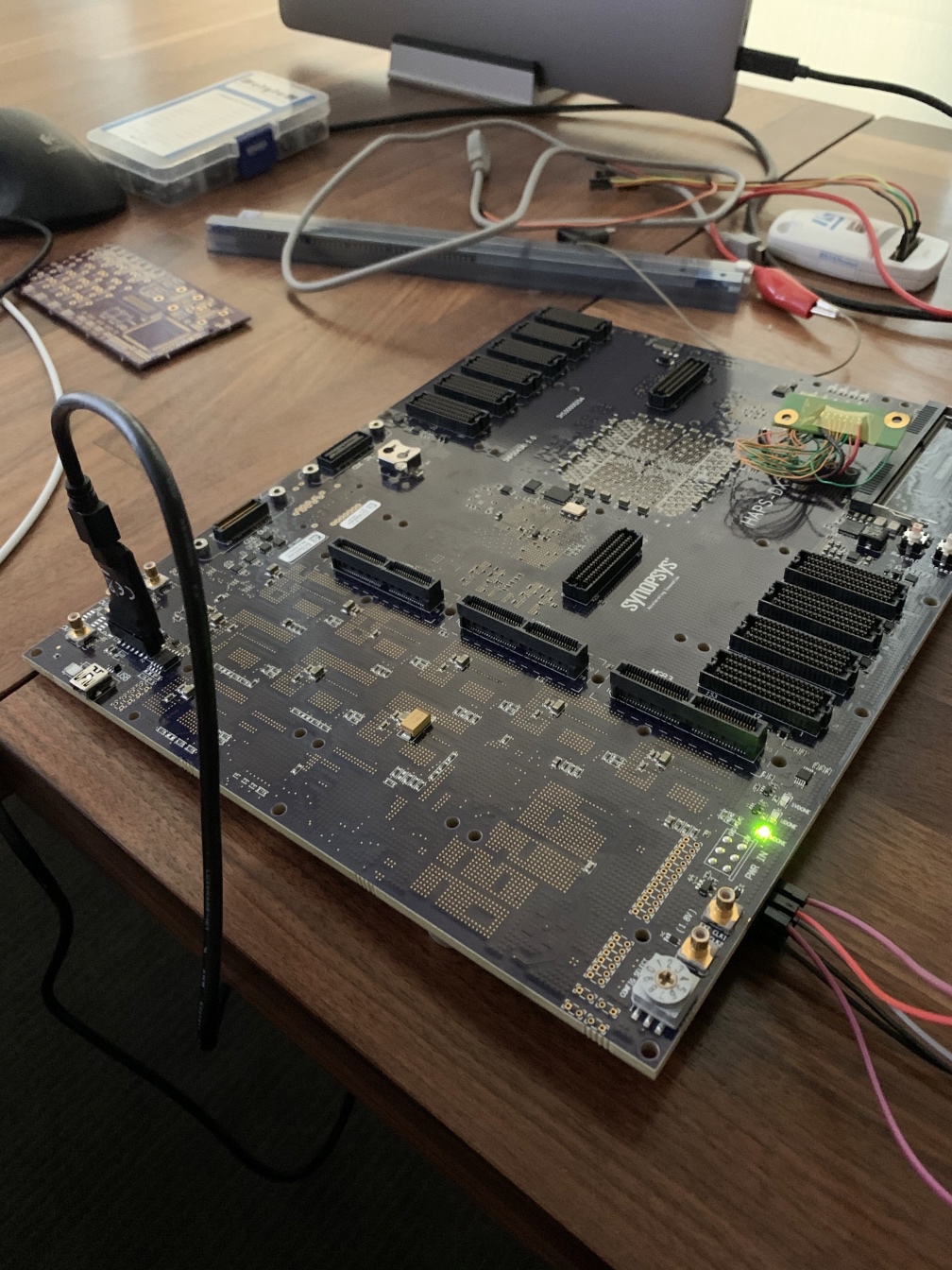
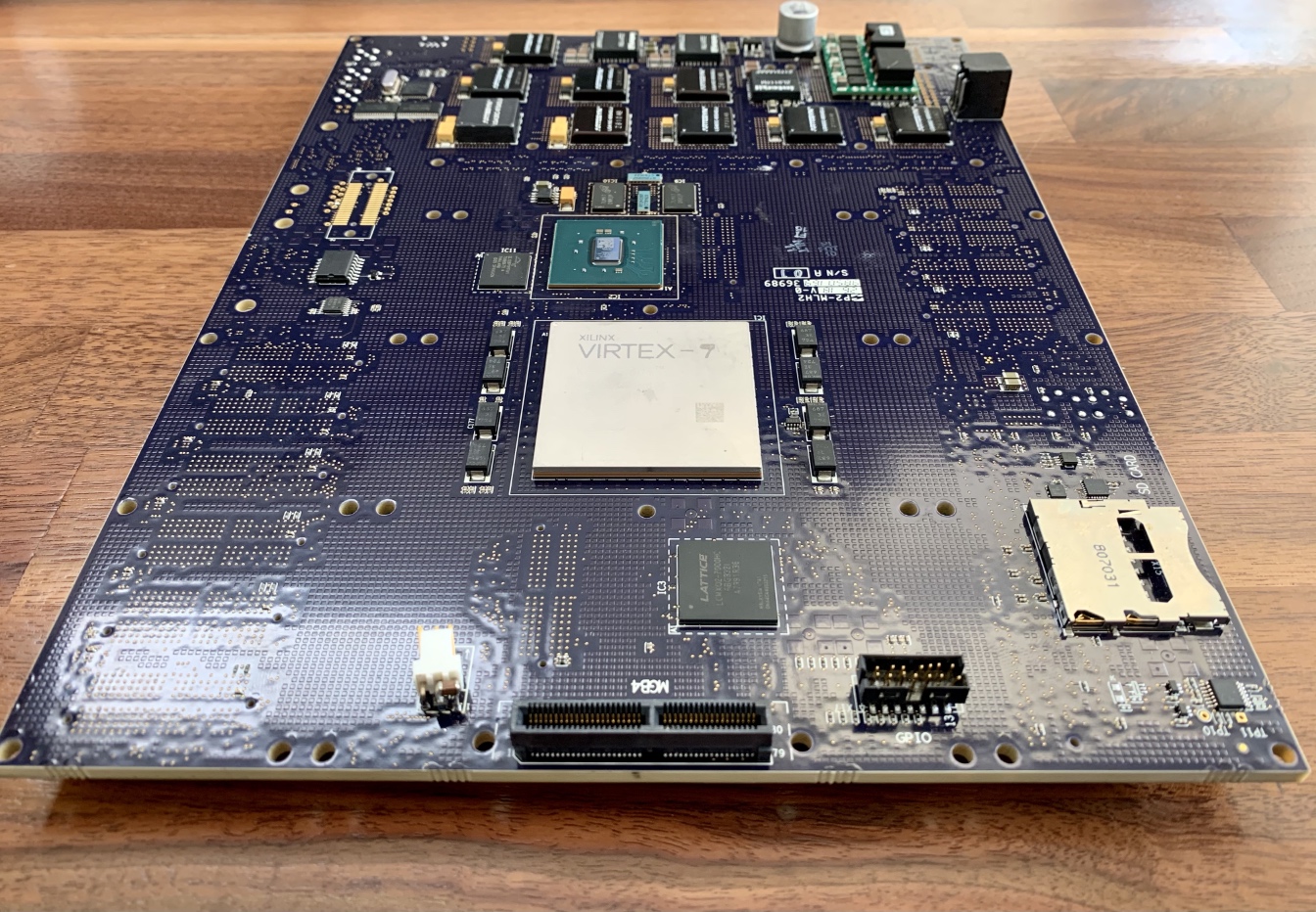 There are three FPGA parts on this board, from back to front: Xilinx Kintex-7 XC7K70T (exposed die on green BGA substrate), Xilinx Virtex-7 XC7VX980T (huge part with the metal lid on the BGA), and a Lattice MachXO2 LCMXO2-7000HC (molded BGA toward the bottom).
This HAPS-DX7 board was originally an “affordable” (> $20k) ASIC prototyping platform for validating IP blocks or other smaller designs. Documentation on the monster is scarce, limited to one marketing-speak heavy PDF that they call a “datasheet”. From what I understand on the datasheet and from what others have told me, this board is tightly integrated with the Synopsys prototyping tools. A proprietary system converts your ASIC block’s RTL into fully instrumented logic with a test harness that can be embedded in the big Virtex part. The test harness then uses a fast data bus to talk to the Kintex part and spit out traces for signals of interest, hence why the Kintex part has a bunch of DDR RAM next to it. A Cypress EZ USB part provides a bridge from the Kintex to USB for spitting out signal traces to a host PC. From the datasheet, it seems like the USB interface can also allow you to run a bus master or slave on the host PC and connect it to logic running in the FPGA. For example, if you are developing an AXI bus peripheral, you could run the IP core full-speed in the Virtex fabric and fiddle with its registers over USB. I’ve never used any Synopsys tools, so take everything in this paragraph with a grain of salt.
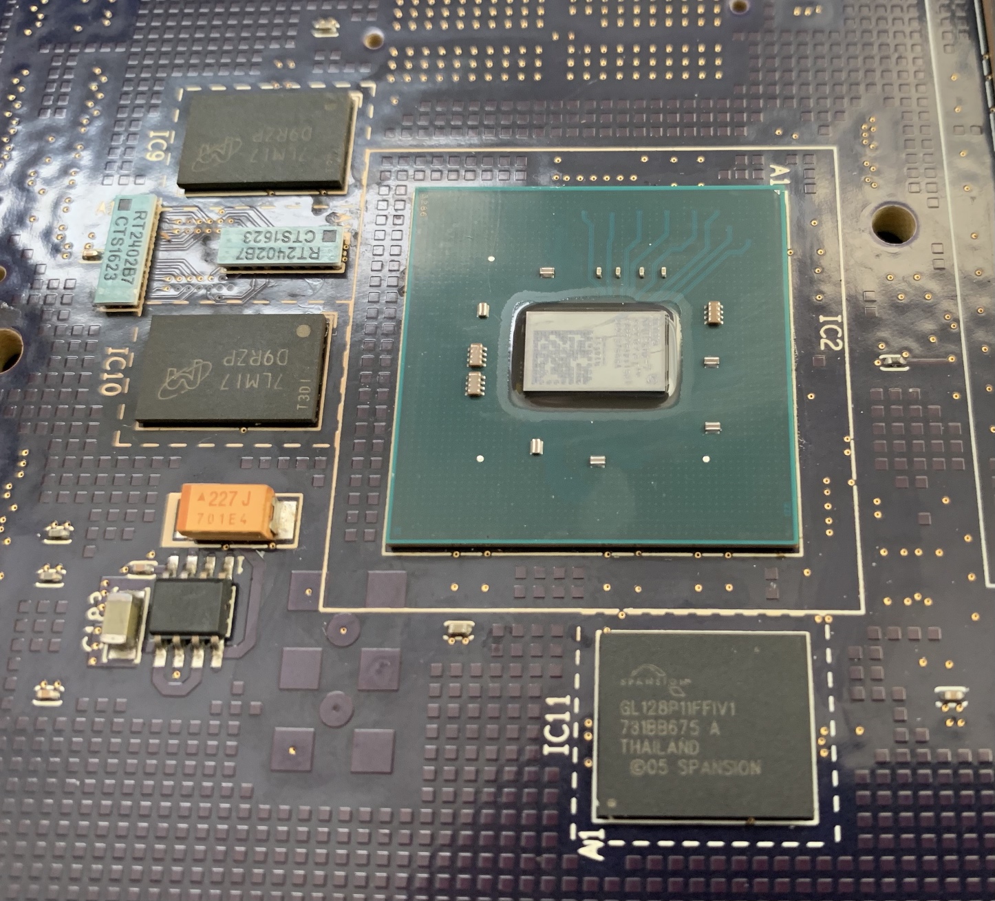
 Left: the Kintex part with a bunch of DDR RAM (2x 128Mx8 Micron parts) for storing traces. It must have an internal soft-CPU, since it has a big flash part in addition to the config flash I found on the backside, likely for storing an OS or at least some kind of big program. Right: the USB interface uses a popular Cypress USB microcontroller and some level converters to connect to the Kintex.
My goals for the board are more limited than full-blown ASIC prototyping with expensive tools. I just want to play around with a gigantic FPGA and see if I can contribute anything to the open-source EDA efforts for Xilinx 7-Series parts. Also, I really want to run Olof Kindgren’s CoreScore on this thing and see how many RiscV cores can fit on one FPGA!
Yes! I would love to see the CoreScore for this beast. I'd reckon perhaps 3000 cores should be possible. Happy to help out
— Rude Olof the rasta reindeer (@OlofKindgren) December 29, 2020
Yes, it can use 3000 cores in a mesh network-on-chip to accomplish the computationally intensive task of... blinking one LED. Necessary? No. Satisfying? Very.
— Craig Bishop (@craig_jbishop) December 29, 2020
The first step on any unknown FPGA board is to find a JTAG port. What could have been a fun challenge was spoiled by the block-lettered “JTAG” label in silkscreen above a standard Xilinx 2mm pitch header. While no fun, that connector is incredibly convenient since my Digilent JTAG HS3 will fit right onto it without an adapter. So, it should be easy right? Hook up power, whack an adapter on the JTAG port and away we go!
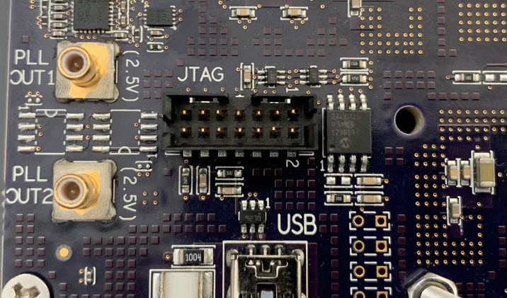 Very clearly labelled and convenient JTAG port
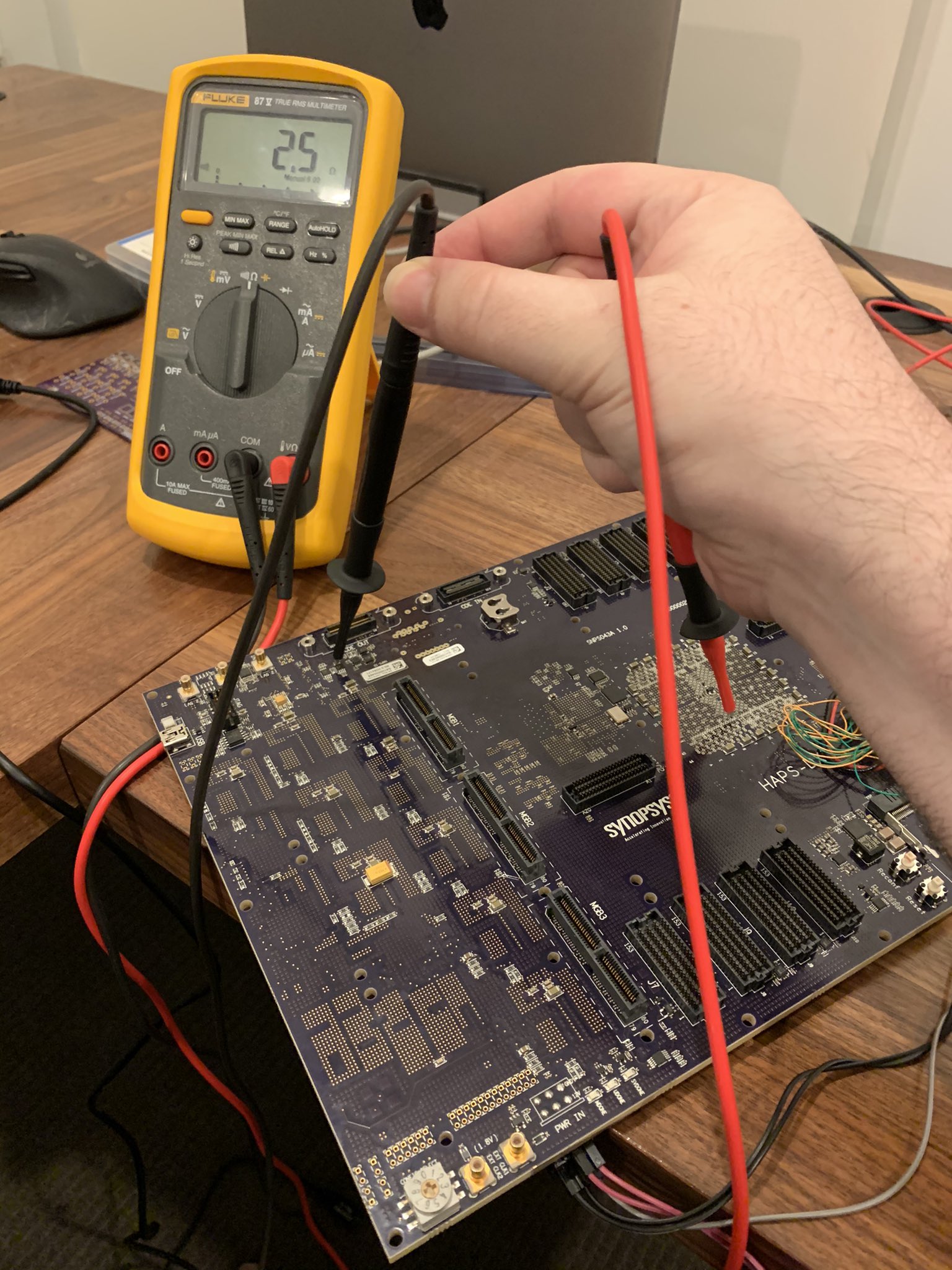
 Left: bench supply showing quite high idle power draw (> 7 watts!). Right: green LED means the board is on, right?!
If it seems too good to be true, most of the time, it is. The JTAG port on this board was no exception. Vivado’s HW manager found the JTAG adapter, but did not detect any components attached. Thinking that I could possibly have some weird driver or configuration issue, I also tried out OpenOCD. During startup, OpenOCD will dump the IDs for anything it discovers on the scan-chain. Again, nothing. This was going to be more difficult.
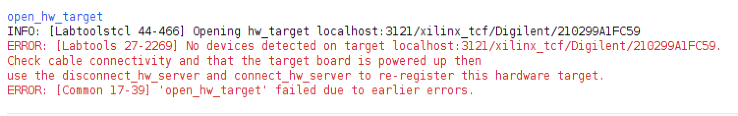 Vivado didn't find any friends on this board
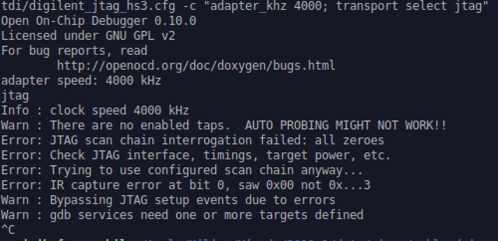 OpenOCD didn't detect anything either; "all zeroes" usually means nothing is powered up or connected
Maybe this clearly labelled and easily accessible JTAG port was a trap? Were the pins even connected to the JTAG pins on the Virtex part? Maybe the Kintex and Lattice parts played a role in the JTAG chain somehow.
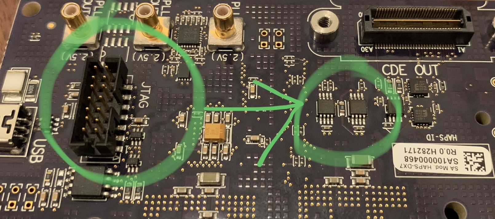
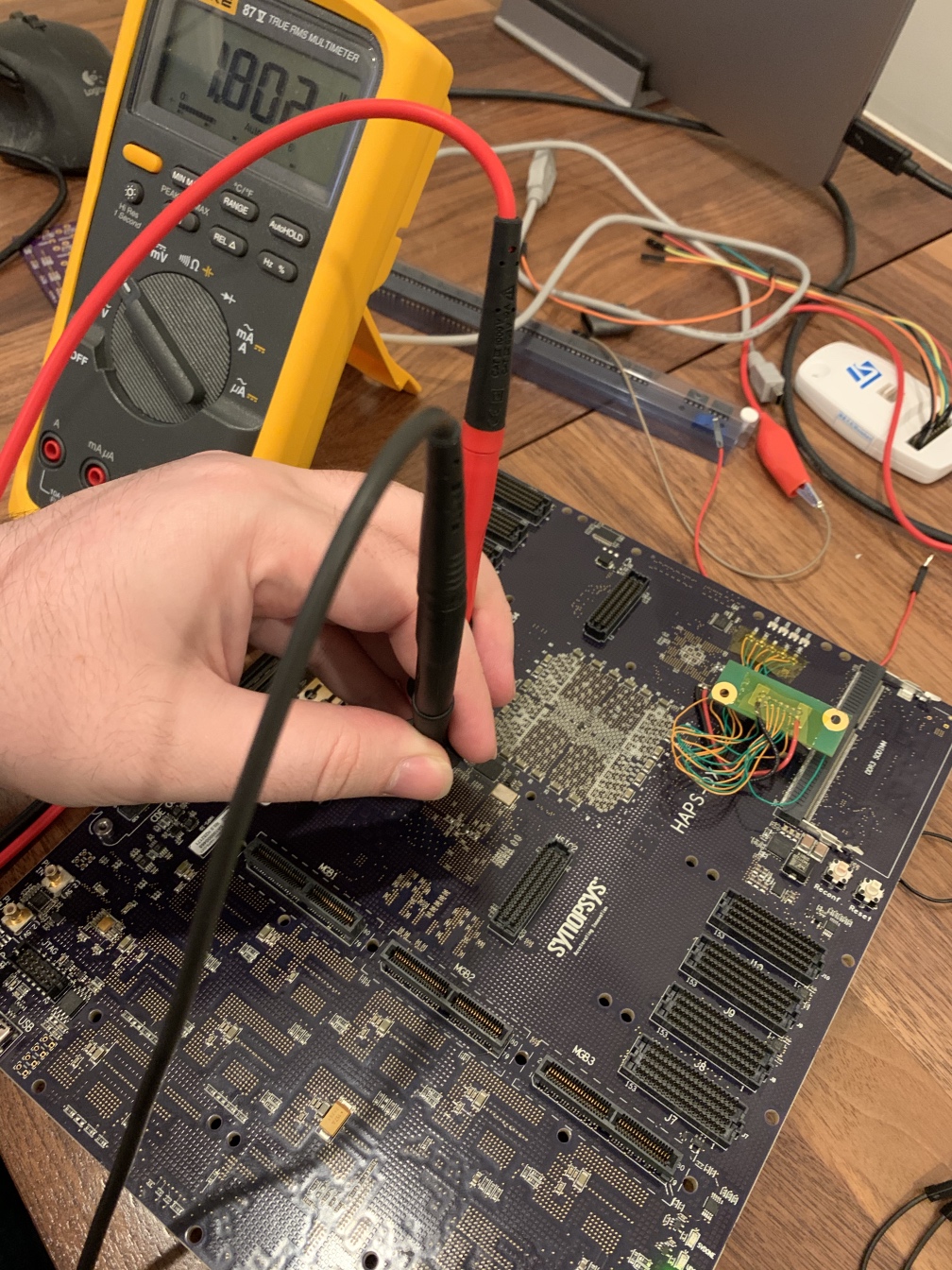
With the BGA diagram open and continuity mode set on my multimeter, I went to town probing away to find where these JTAG signals led. They were indeed not directly connected to the Virtex part, but through some smaller little chips near ports named “CDE IN” and “CDE OUT”. The part numbers are not quite clear, so I still haven’t figured out if these are level shifts or multiplexers. I wouldn’t think you’d need level shifters on a JTAG port, since JTAG will use the voltage level applied to the VREF pin. Maybe they are multiplexers to optionally allow a master board to access the JTAG port? Either purpose, these little chips were not powered up either!
 The JTAG signals on the Virtex BGA are not directly connected to the labelled JTAG port, but to a collection of smaller chips that could be multiplexers or level-shifters
 These little ambiguous chips were in the signal path from the JTAG port to the Virtex-7. They have the Analog Devices logo and are marked "S" "1S".
Without power to the small ambiguous chips or the Virtex, there was no hope of JTAG connectivity. The fundamental theorem of electronics troubleshooting seemed to apply here: “thou shalt check power” (known in other industries as “is it plugged in?”). This case was no exception, the Virtex wasn’t plugged in! Probing the decoupling caps on the Virtex showed no voltage on any of the rails. However, when I probed the Kintex and Lattice parts’ voltage rails, there was non-zero voltage. Looks like one of the other FPGAs controls the power for the big Virtex part.
 The Virtex part measures near zero on all rails, while the Kintex part is happily powered up.
Finding the power management section of the board was pretty straightforward, since it has more than $100 worth of integrated DC-DC power modules. FPGAs have many voltage rails, so it’s not surprising to find a ton of DC-DC converters. The power requirements for Virtex parts are well beyond anything I’ve previously worked on though, so the scale was still impressive. The big module that looks different than the rest is a PTH08T250 (thanks @rombik_su!), and since it has the highest current capability, it was most likely the Virtex 1V core supply. The three modules that don’t look like the rest were Intersil ZL9117M parts, with adjustable output voltage controlled over I2C. The rest are a mixture of ARTESYN LGA03C, LGA10C, and LGA20C modules with fixed outputs.
When the board was powered up and I probed each power module, the arrangement became clear. Three enabled rails provided 1V, 1.8V, and 2.5V to the Kintex. Another enabled rail provided 3.3V to the Lattice MachXO2. The rest of the rails, including the adjustable rails, were all shutdown using the inhibit or enable pins. These must be the Virtex power rails!
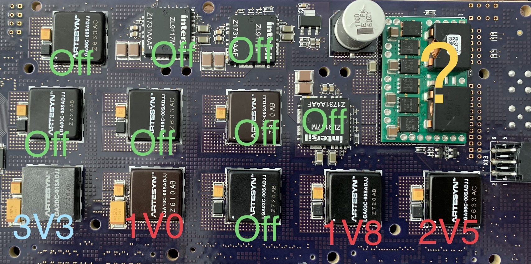 It takes quite a few power modules to supply all these FPGAs! The red labelled modules are for the Kintex, the blue labelled module is for the MachXO2, and the rest are for the Virtex.
Since the Intersil modules have exposed pins to probe, I started with those. As expected, the enable pin on each had a pull-down resistor to disable the module on startup. Most likely, the modules are controlled by one of the FPGAs and the resistors keep them shut-off while the IOs are still tri-stated. To follow the enables, I used a tried and proven strategy: “flail around with a multimeter probe in continuity mode and wait for the beep”. Since this board was originally made for prototyping, the PCB designer kindly left all of the vias un-tented (not covered in soldermask). So, I could just drag the multimeter probe across the sea of vias under each FPGA and hope for a beep. I eventually gave up on the Kintex part and moved to the Lattice MachXO2 part, and founds beeps for all of the enables there.
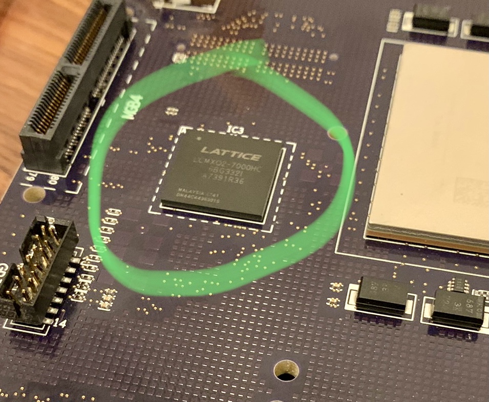 Left: since all the vias are un-tented, probing was quite easy and quick. Right: this LCMXO2-7000HC seems to control all the power.
Eventually, I traced all of the power modules, and some general purpose debug LEDs, to the Lattice FPGA. Even though the ARTESYN modules don’t have exposed pins, it was pretty simple to find the enable and power good signals on the backside of the board. Each module had a via to a pull-down resistor and another via connected to a pull-up resistor. The module datasheet says the enable input is active high, so the pulled-down signal is definitely the enable. The pull-up resistor on the other signal was a strong hint that it’s an open-drain power-good output. You can see the results of the mapping in this constraints file.
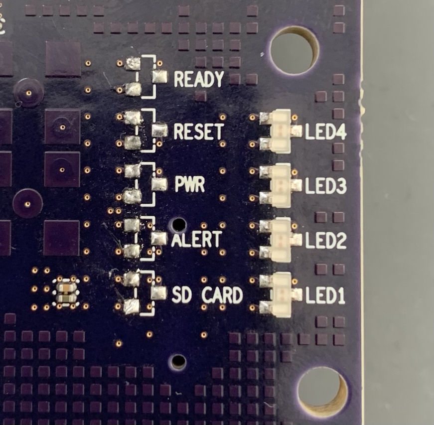
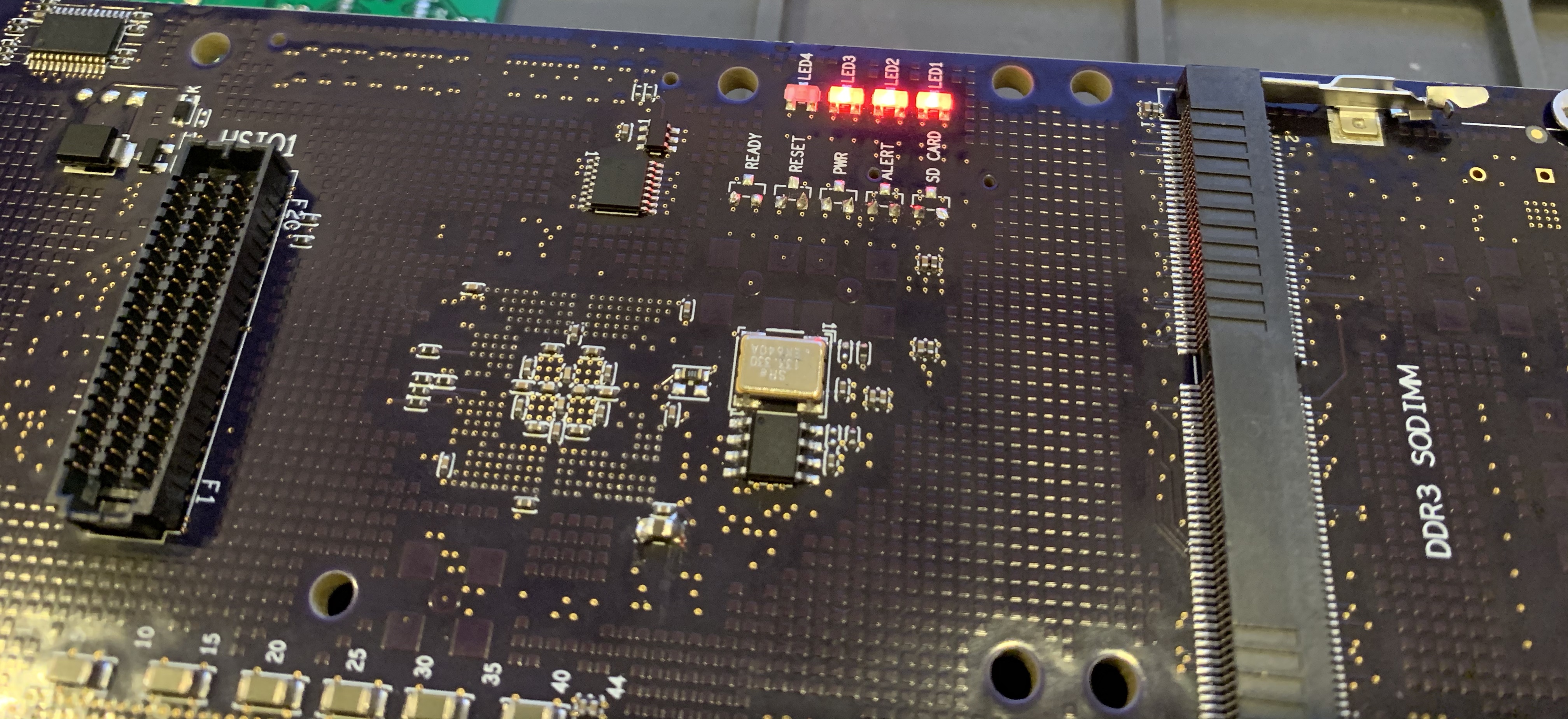
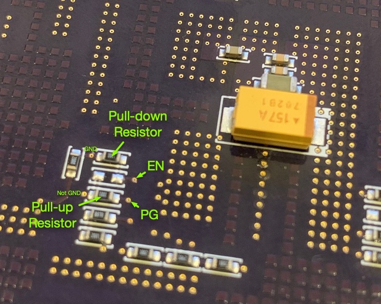 Left: general purpose debug LEDs and other status LEDs go straight to the MachXO2 part. Right: the enable pins on the modules are pulled down and the power-good open-drain outputs are pulled high.
To boot the Virtex rails up in the right order, I’d also need to know which power modules connect to which rails. So, again I pulled up the BGA diagram and probed the power modules outputs and power pins on the BGA to match the two.
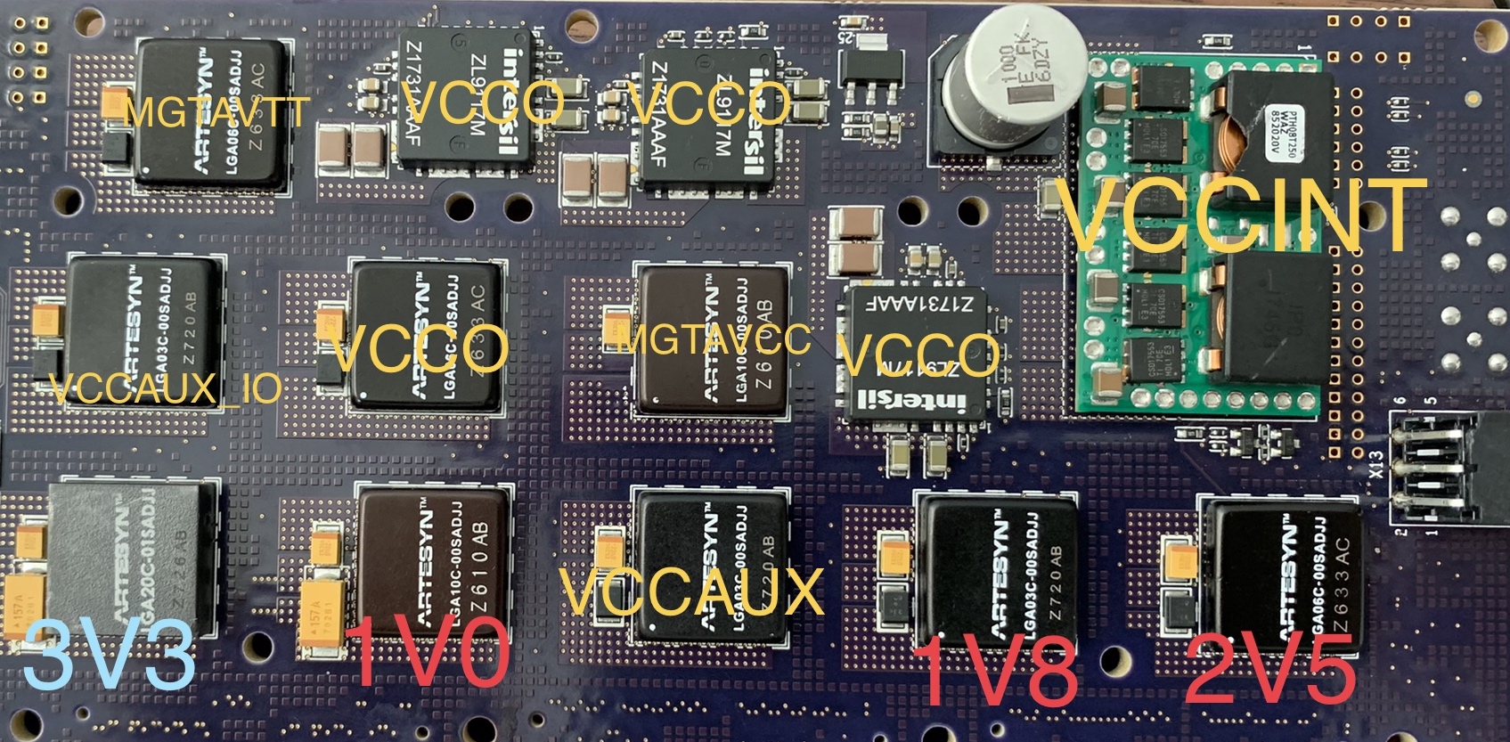 All the yellow labels are Virtex-7 power rails mapped to DC-DC converters
Well, all of this means that the Lattice MachXO2 part is critical to powering up the Virtex, and it’s running a bitstream that I have no clue about. The easiest path forward would be replacing the MachXO2 bitstream with a simple design that powers up the rails in the right order. Understanding an existing bitstream is not an easy task at all–it’s not like disassembling a binary at all!
To override the MachXO2’s behavior, I’d need its JTAG port though. Luckily, the designers of the HAPS-DX7 don’t seem to have prioritized obfuscation, and the port they used to do the initial programming is readily visible. These kinds of ports for spring-loaded contact connectors are really common for flashing a board before it’s shipped. Probing with a multimeter in continuity mode again, I found the JTAG signals for both the Kintex and the Lattice part.

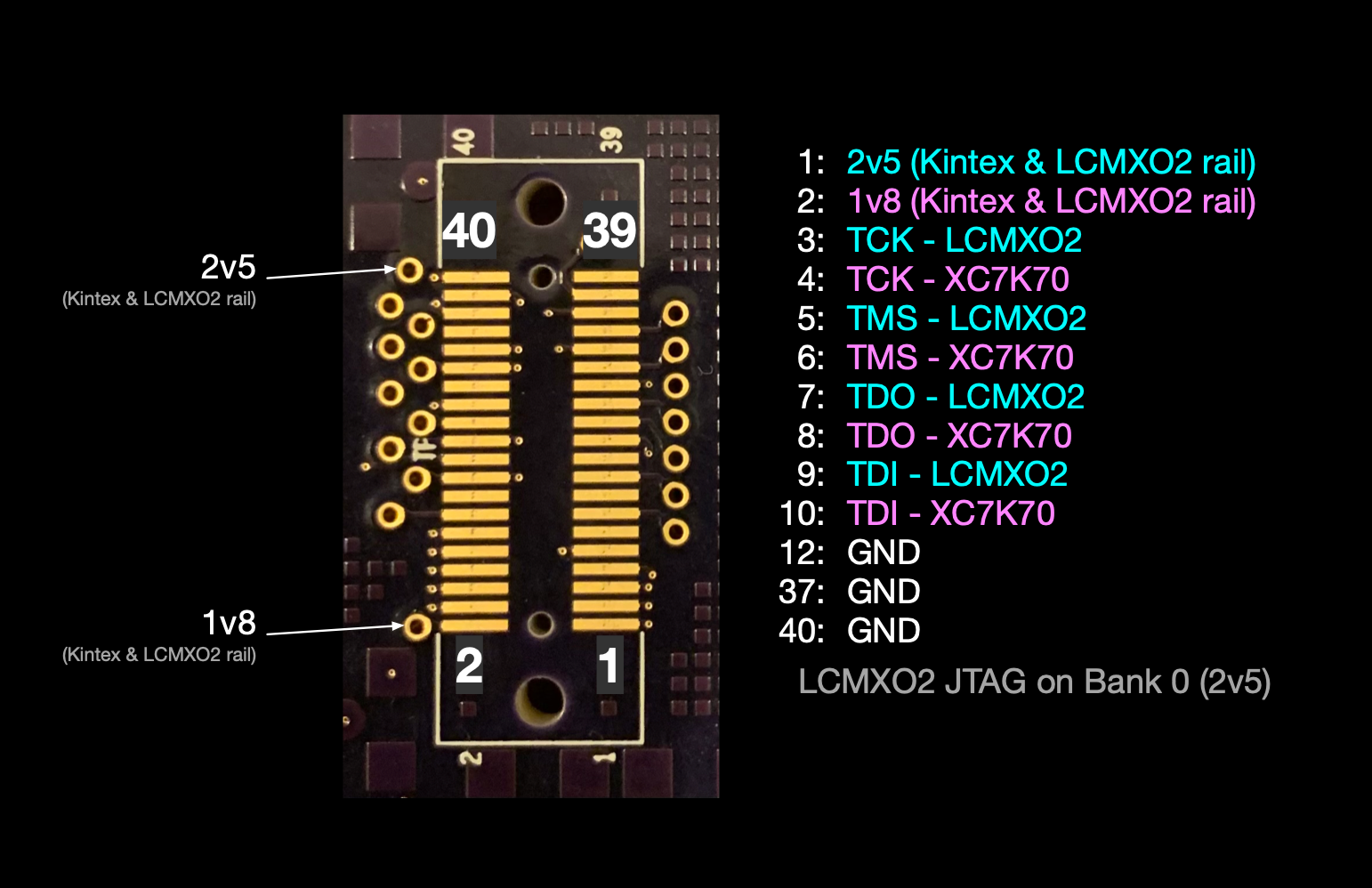 The JTAG ports for both the Lattice MachXO2 and the Kintex part lead to this unpopulated connector footprint. The pin-out probably has more useful signals, but the diagram shows what I found so far.
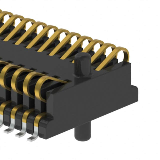
Rather than bodge some wires onto the nice gold-plated pads, I decided (with some urging) to design an adapter board for the job. The prevalence of Samtec connectors across the whole board was a pretty good hint that the spring contact connector would also be a Samtec. Yup: Samtec Inc. FSI-120-03-G-D-AD. A little KiCad-fu later, and I had an adapter board on the way.
The adapter board design is available on GitHub here: https://github.com/craigjb/DX7-JTAG
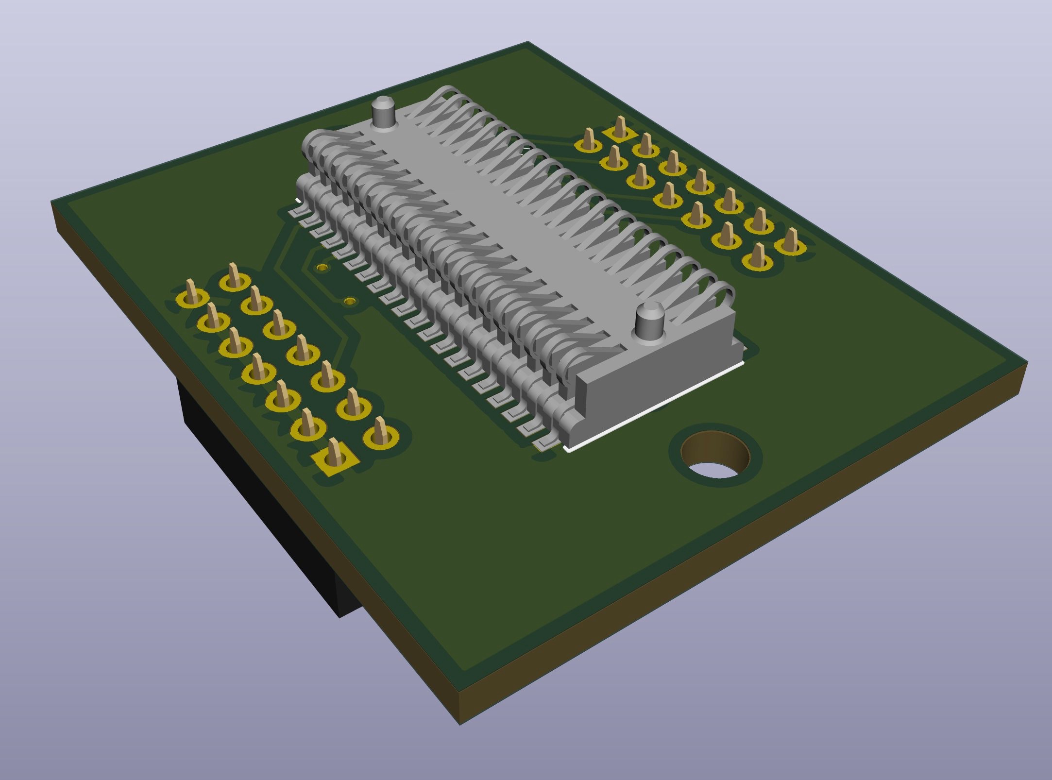 The adapter board was hastily designed and sent off to the fab with some SnapEDA footprints! I am really liking that site now (not affiliated).

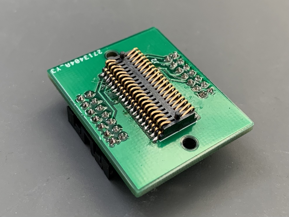
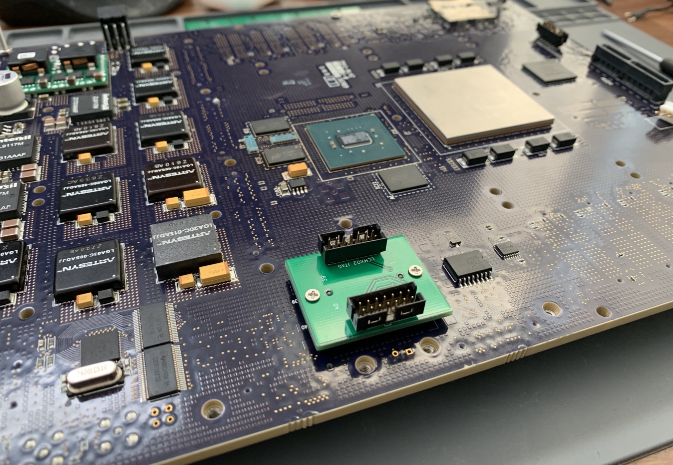 The spring contacts press onto the gold-plated header pads and two M2 screws hold it in place.
With the board powered up, and the adapter plugged in, I was able to confirmed JTAG access for both the Kintex and MachXO2 parts. Almost there!
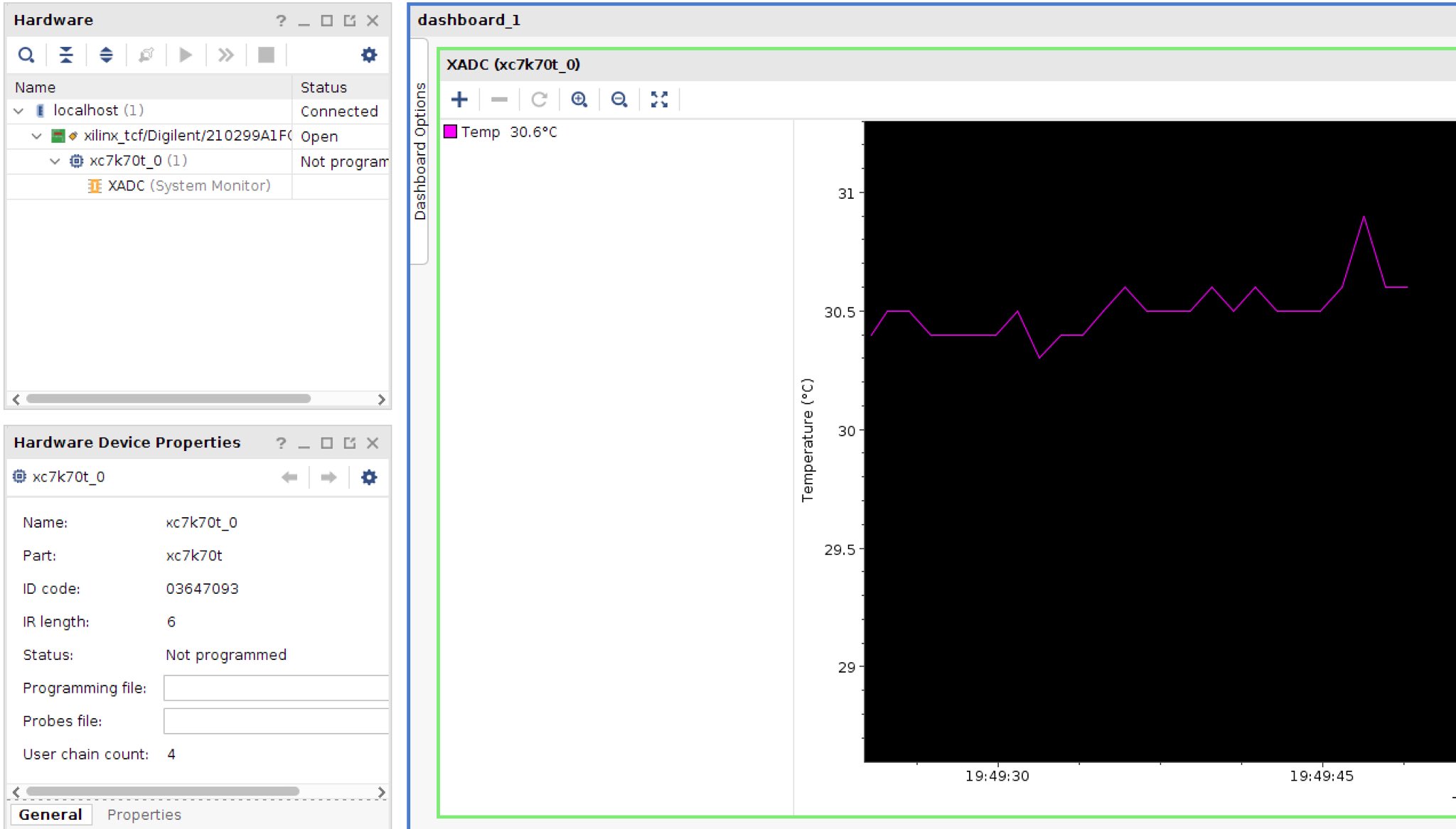 Vivado's HW manager showed the Kintex part detected over JTAG. The Vivado GUI also shows you an internal temperature plot measured on the built-in ADC.
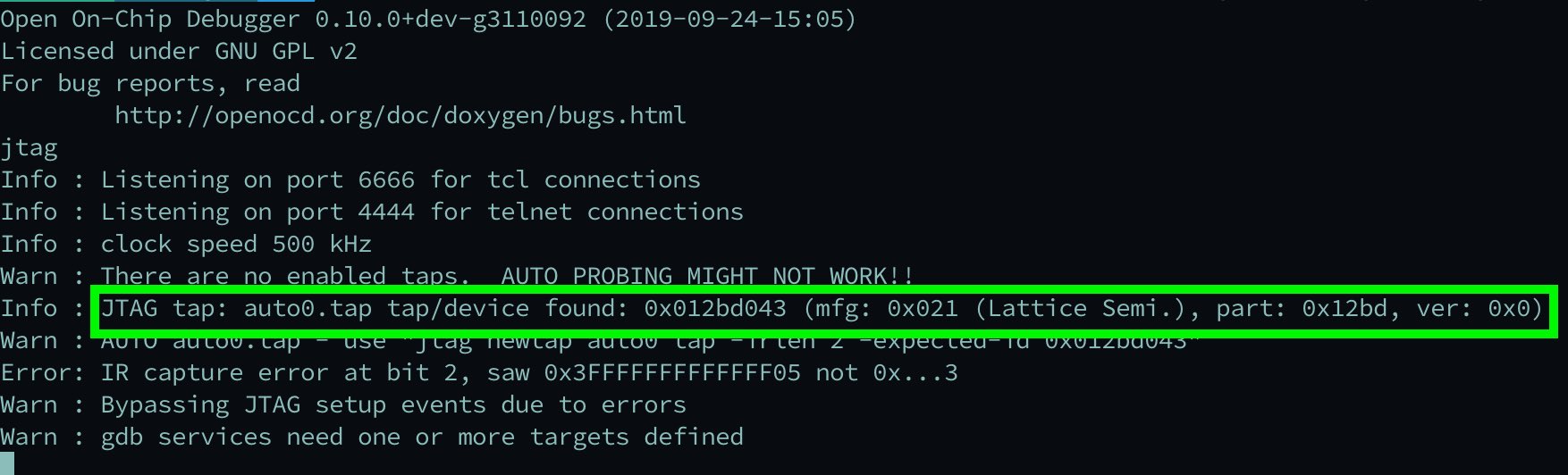 OpenOCD even knows manufacturer JTAG IDs well enough to tell you it's a Lattice part! I'm not sure if OpenOCD can program these parts though.
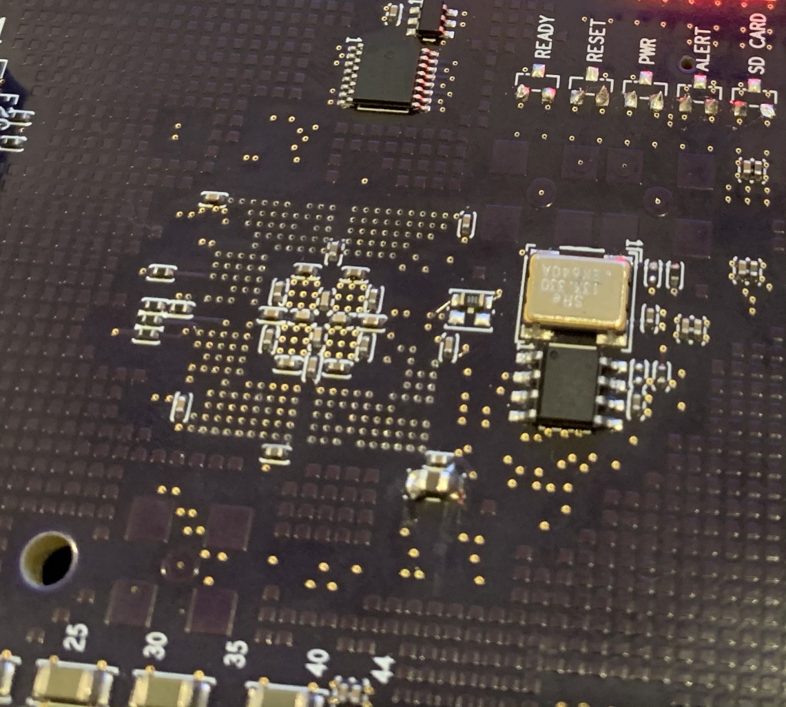
Finally, it’s time for a little Verilog. At first I was a little concerned with the clock situation. For the MachXO2 to run anything, I’d need a clock, and the oscillator closest to it was not connected to it. There’s a 133.33 MHz oscillator right next to the part and run through a clock buffer, but none of the outputs go to the MachXO2.
Taking a break from probing around, I started reading the MachXO2 datasheet and found that the part actually has an internal oscillator with a configurable output frequency! That makes things much simpler.
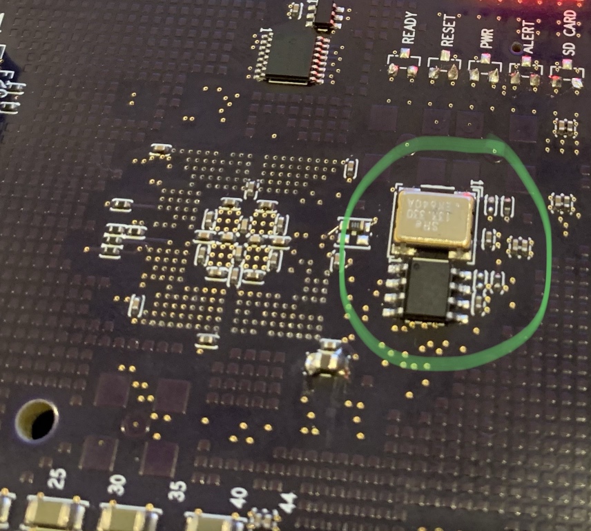 This 133.33 MHz oscillator goes to the Virtex, not the Lattice part
With a little bit of Verilog and some constraints, we have power, mostly! I routed each LED to a combined (and’ed) power good signal. The first three stages come up fine, but the last stage has the adjustable Intersil converters on it (for VCCO levels). Unfortunately, it looks like they don’t have a default voltage level saved. JTAG should work just fine without those rails though.
 The Verilog module has four stages, with the combined power good signal for each stage routed to an LED.
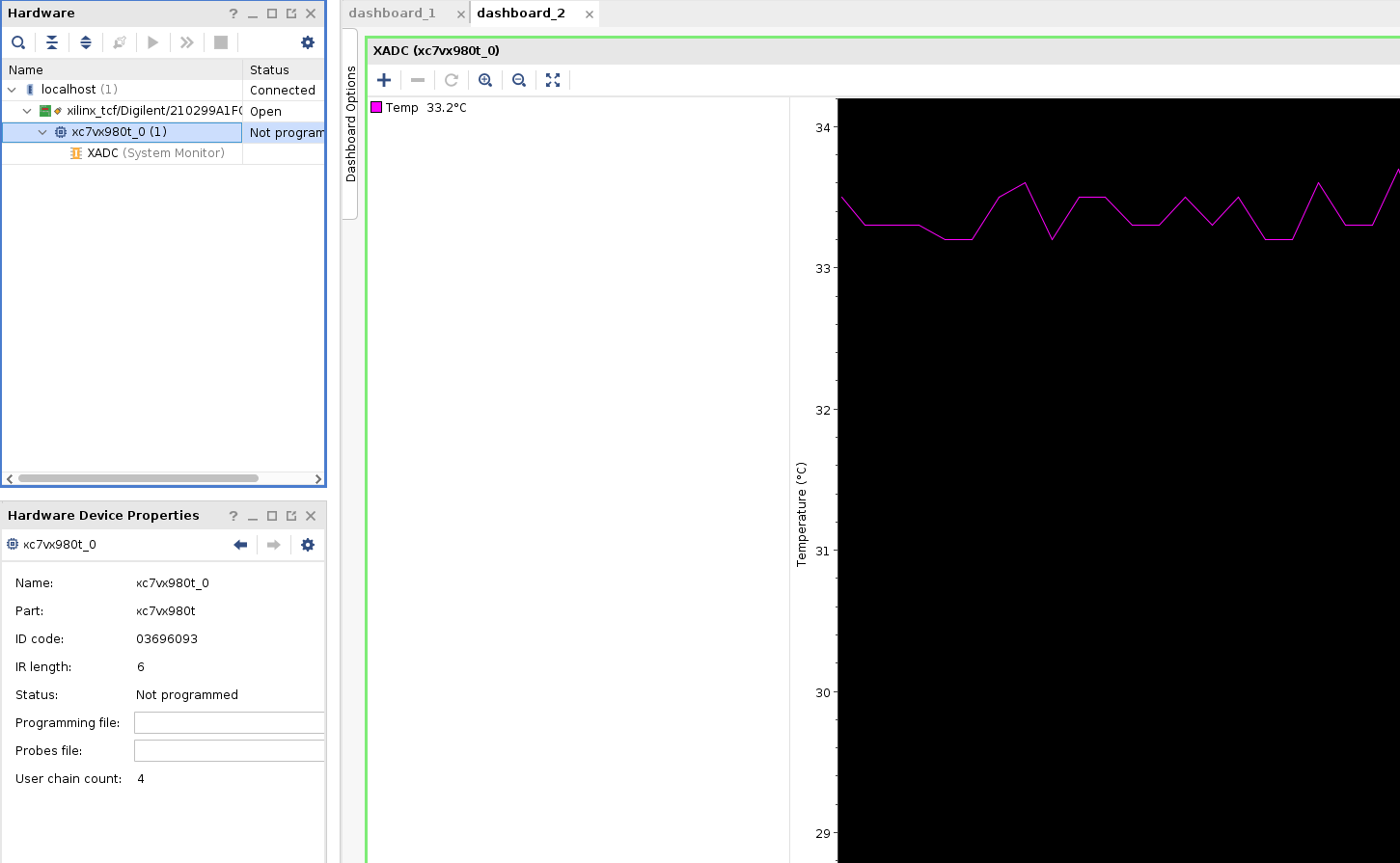 Vivado showing the XC7VX980T on JTAG! Woo!
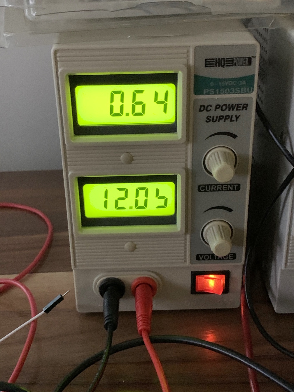
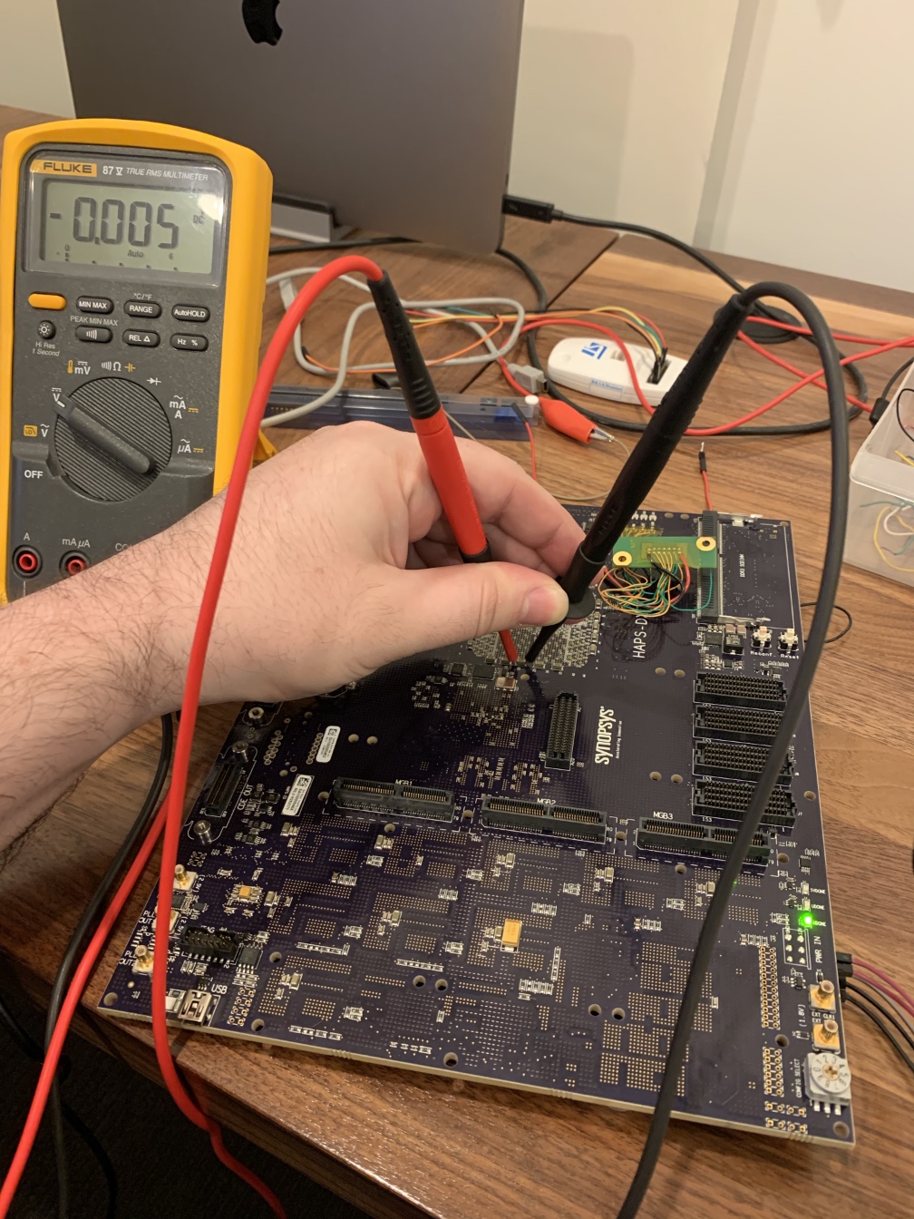
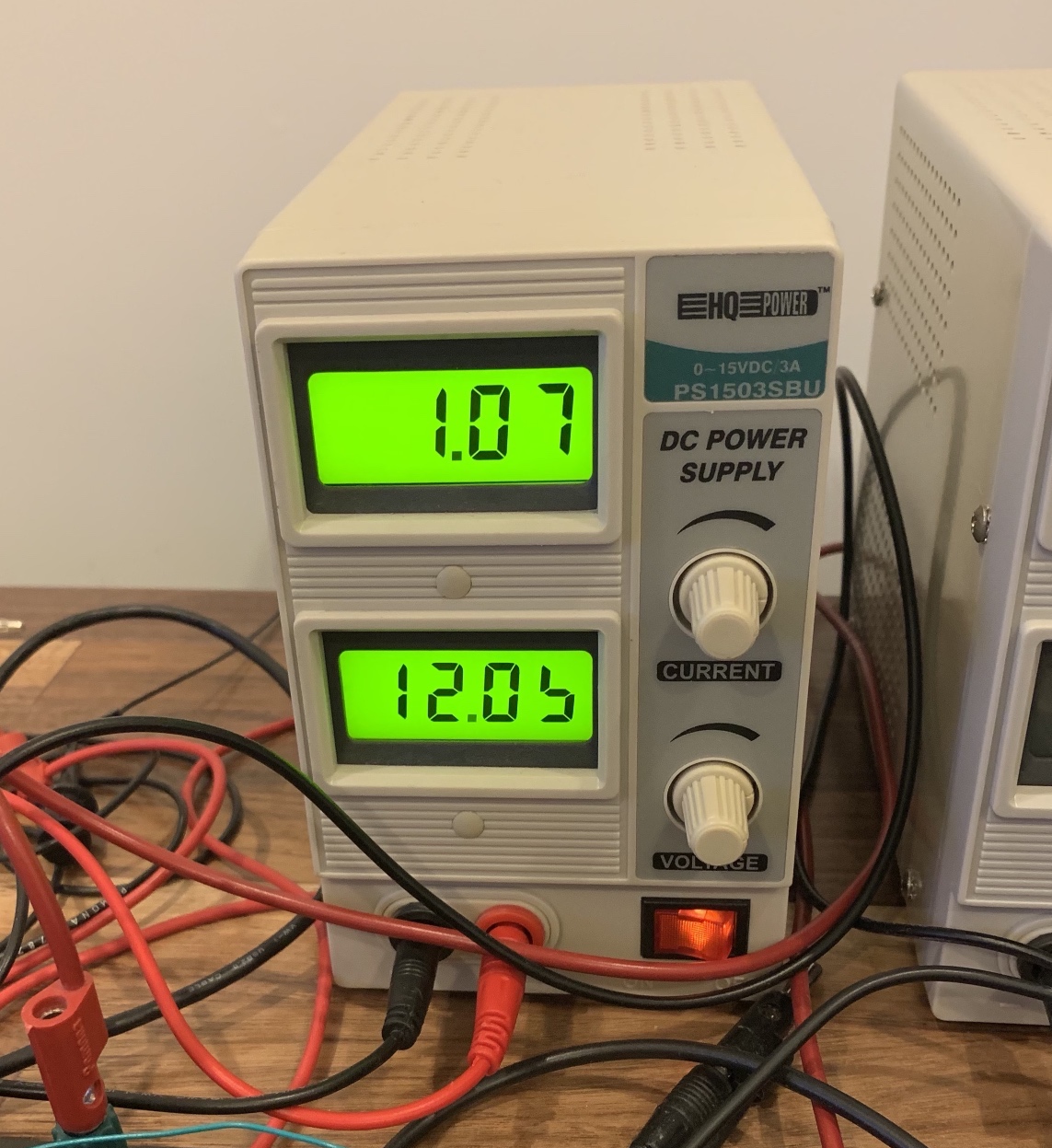 Left: Digilent HS3 connected to the clearly labeled JTAG port. Right: idle power went up significantly with the Virtex powered on, over 12 watts!
That’s a win! Vivado confirms the part ID as a XC7VX980T. I wish it’d show the speed-grade, since the packages with the 2D code don’t have the speed-grade printed. But hey, the gigantic part is accessible now!
I still have quite a bit of work to make this a usable dev board though:
- Find a clock for the Virtex
- Configure the remaining adjustable VCCO DC-DC modules
- Trace some IO to some connectors, maybe the GPIO header first
- Trace the DDR3 SODIMM connector
I’ll definitely post some more as I go. I’ve also been posting things as I go on Twitter.
GitHub links:
- Constraints file for the MachXO2 and Verilog to boot the power supplies: https://github.com/craigjb/BFFPGA
- KiCad design for the adapter board: https://github.com/craigjb/DX7-JTAG
Other links: