
Gameslab first steps
I bought one of the PSP LCD screens from Sparkfun forever ago, planning on building some kind of game console-like device with it. Slowly, I accumulated more hopeful parts, like the PSP-style thumb-sticks and a touchscreen that fits the LCD perfectly. All these parts are screaming at me to build something cool, so I’m going to build an FPGA based, hand-held game console. From scratch.
Building a hand-held console is going to be very different than my previous game console builds, since the small form-factor requires designing the mechanical and electrical components together. I’m not really a fan of the 3D-printed look for project cases, so I want to use some kind of milled aluminum for the front and back panels. Ideally I can have some engravings and maybe even color fills. I might still use 3D-printing for building some side-walls or grips pieces to make the metal edges more comfortable.
Since I have previous experience with Xilinx FPGAs (specifically the Spartan 6 series), I decided on a Spartan 6 part: the XC6SLX25. This is the largest logic cell count available in a decently solderable package. The FTBGA package is 1mm pitch, which is doable with OSH Park PCBs and a toaster oven. Other than the FPGA, the console requires battery charging, power regulation, memory (probably DDR), LCD interface, touchscreen interface, audio (headphones and maybe speakers), thumb-stick interfaces, SD card, some buttons, and maybe Wi-Fi.
Some 3D CAD modeling
I decided to model most of the mechanical components using SolidWorks (it’s what I know how to use). I’ll need to position all of the components before I can design the PCD. The LCD connectors, thumb-stick connections, buttons, battery connectors, power connectors, and SD card slot all depend on the overall mechanical layout. And, there is not going to be a lot of spare room.
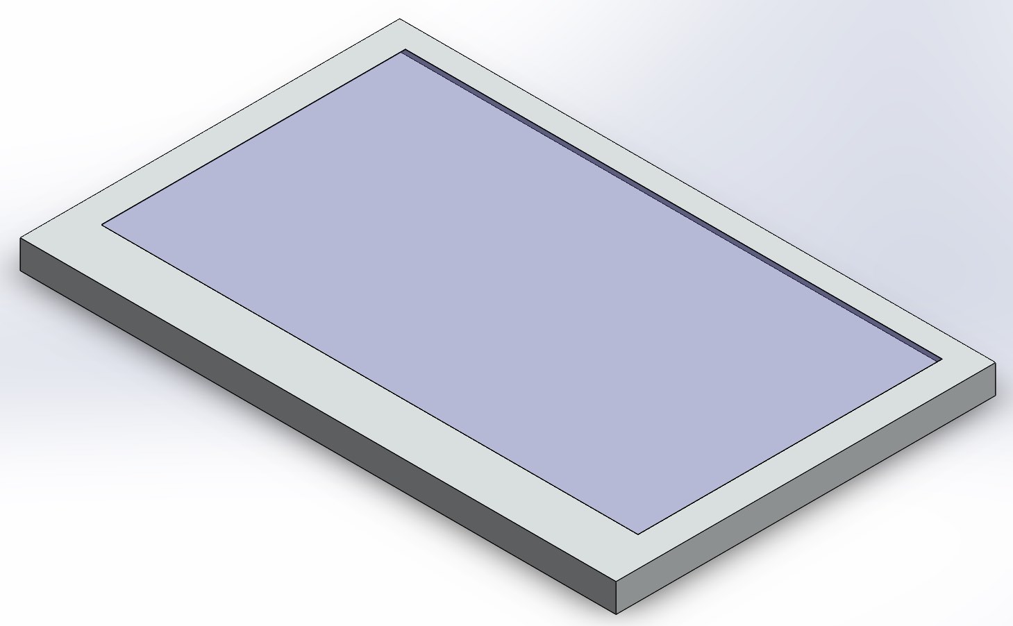
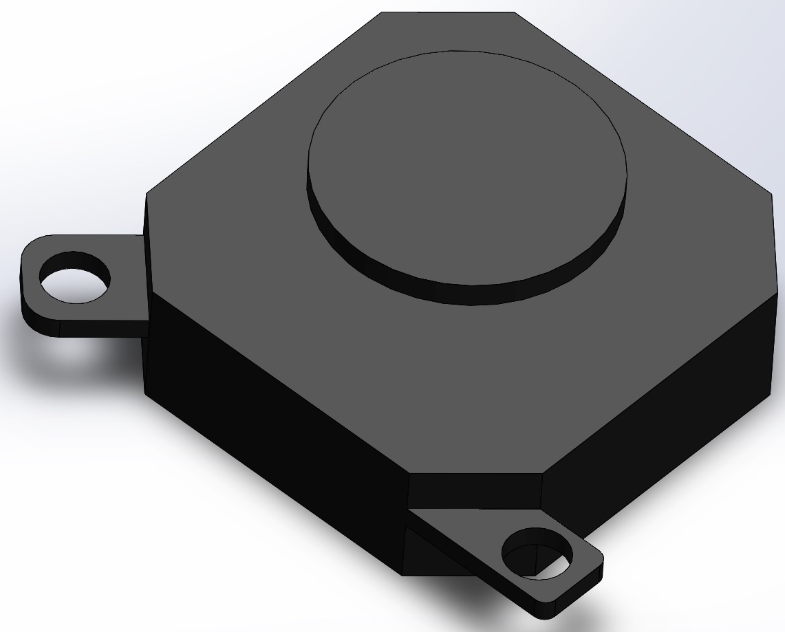 Left: the LCD CAD model; right: the thumb-stick CAD model.
Planning
Several parts of the electrical design will be tricky; I expect designing the FPGA power regulation and DDR interface will be the most painful. To alleviate some of the pain, I’m using the Digilent Atlys board schematics as a reference. However, I have to be careful, since the Atlys was designed to run off of a wall wart. The Gameslab needs to have decent battery life running on rechargeable batteries. For example, the DDR2 address lines on the Atlys are parallel terminated with ~50 Ω resistors.There are 13 address lines, and each line swings between 0 V and 1.8 V. Therefore, each address line will have a DC power dissipation of approximately 16.2 mW. Together, that’s 210 mW! I plan on using one or two lithium polymer batteries, maybe 2000 mA each at 3.7 V; for one cell, that’s 7.4 Watt-hours. I want 4-5 hours of battery life, so system dissipation should be around 1.5 W, and 210 mW is 13.4% of that–just for termination!
The Atlys board uses some really nice Linear Technology switching regulators for the 3.3 V rail, 1.8 V rail, and the 0.9 V DDR2 termination reference. I don’t feel like paying $7 per regulator, so I’m going to do some shopping. I already found a replacement for the LTC3413 (the DDR2 0.9 V reference regulator). On Digikey, the LTC3413 costs $7.94 per unit (in onesey-twosey quantities). The NCP51199 DDR2 termination regulator from ON Semi costs just $0.70.
I’ve also given the FPGA configuration at startup some thought. FPGAs are designed to load their configuration from an external memory (SPI or parallel flash typically) at startup. However, wouldn’t be interesting if every game could have completely custom hardware? That’s why I’m looking at including a microcontroller to interface with the SD card and perform the FPGA configuration and re-configuration. The microcontroller can load a default FPGA configuration that will present a game selection screen, and then once a game is selected, the FPGA will communicate with microcontroller, instructing it to re-configure the FPGA with the selected game image. The XC6SLX25 has 6,440,432 configuration bits (The total number of configuration bits was hard to find. It’s buried in this document at the end of page 75), and with a maximum configuration serial slave clock of 80 MHz, that would take 80 ms to reconfigure–about 5 frames at 60 FPS.
Since power is going to be a big design issue, I thought I’d do a quick estimate of the likely power consumption. I have a previous FPGA design for the Atlys board that contains a Microblaze soft processor, DDR2 interface, and an HDMI output. Since the Atlys board uses an FPGA almost twice the size and the design is much higher speed, the estimate should be conservative. I used the Xilinx XPower Analyzer, and came up with the values below:
| Supply Rail | Voltage | Current | Power |
|---|---|---|---|
| VCCINT | 1.2 V | 0.370 A | 0.444 W |
| VCCAUX | 3.3 V | 0.108 A | 0.356 W |
| VCCO33 | 3.3 V | 0.022 A | 0.073 W |
| VCC018 | 1.8 V | 0.196 A | 0.353 W |
| Total: | 1.226 W |
Obviously this is going to be pushing the limit of a single 2000 mAh lithium polymer cell. The Gameslab will likely require two of the cells, since 1.226 W eats almost 82% of the power budget already.