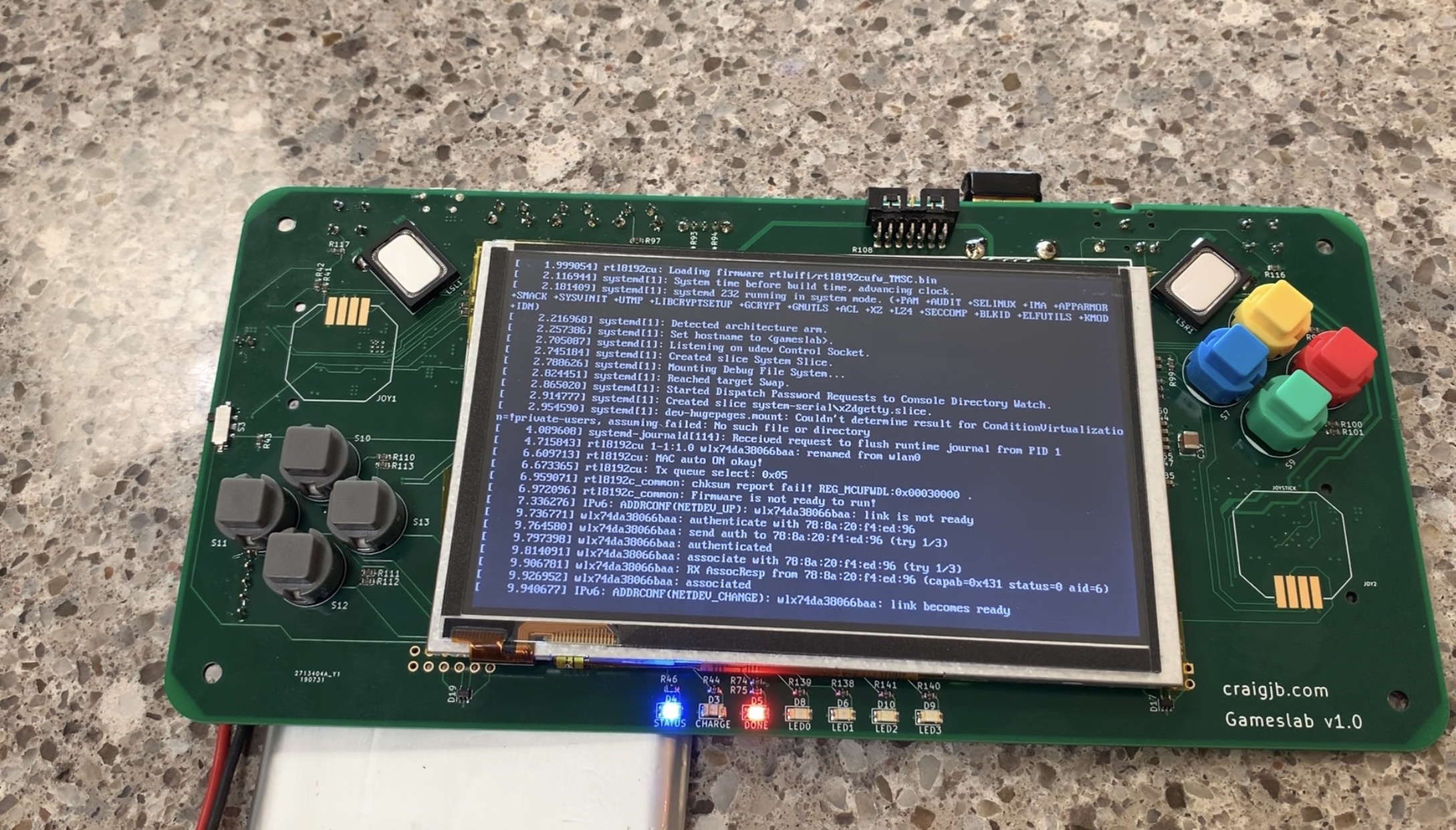
Gameslab project overview
If you went to Hackaday Supercon 2019, you might have seen someone wandering around with a badge that was way too heavy looking. That was me! And that badge was a Gameslab, my FPGA-powered handheld game console. As the blog posts from years ago prove, I’ve been thinking about building Gameslab for a long time, and over the last few months, I have finally done it. In this post, I’ll explain what exactly a Gameslab is (game-slab, as in brick, or unwieldly object that plays games), why I built one, what’s in it, and how I got it working.
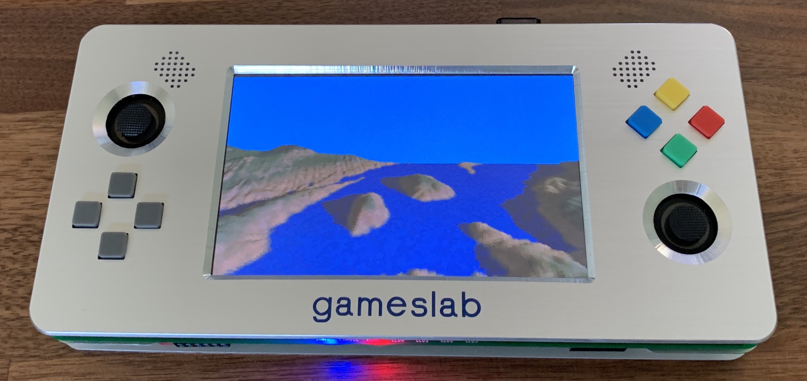 Gameslab running a 3D terrain demo; remember the old Comanche helicopter games? It's the same terrain drawing algorithm in FPGA hardware.
What is Gameslab?
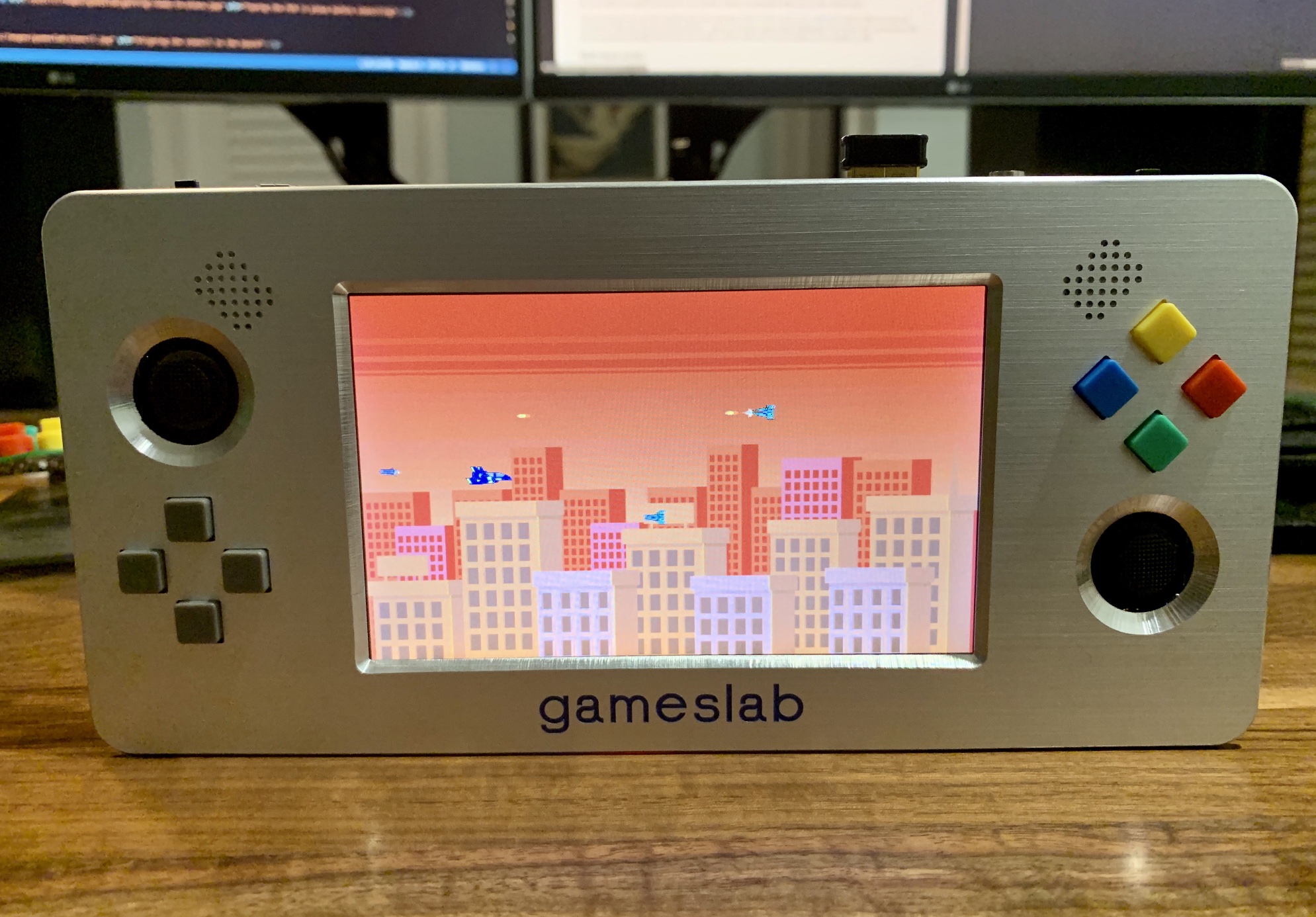
The Gameslab is a custom-designed handheld game console based on a Xilinx Zynq FPGA-ARM Cortex A9 combo SoC. The FPGA fabric means that games and apps can bring their own unique hardware to load into the fabric. For example, a 2D side-scrolling shoooter can load hardware to accelerate drawing and animating sprites on the screen. Or, a Gameboy emulator could load a Gameboy’s CPU and peripherals into the FPGA fabric to “become” a Gameboy rather than emulating it in software.
The Gameslab was designed using the open-source KiCad (even the painful, high-speed DDR3 interface). An STM32L0 onboard runs embedded Rust firmware based on the RTFM RTOS. The Zynq bootloader is a ported brnach of Das U-Boot, using the secondary program loader (SPL) to avoid using Xilinx’s FSBL. The bootloader loads a custom-compiled mainline Linux kernel version 4.12 (not Xilinx tree) with drivers for the custom hardware in the FPGA fabric. A micro-SD card contains a custom-built Debian root image: SlabOS :) . The game below and the terrain demo above are userspace apps that I built in Rust to test out hardware in the FPGA fabric.
Why Gameslab?
I learned to program when I was a kid because I wanted to make games (Visual Basic 6, woo!). The internal mechanics that made games work always fascinated me more than the games themselves, and eventually I found the hardware that the games ran on was even more interesting. Games tend to push limited hardware to the max to generate special effects or realism that the competition before you didn’t figure out yet. Years ago, I built the Gamesphere, a console based on an ARM CPU, dual-port RAM, and some microcontrollers. Since then, I started working with FPGAs (awesome talk if you want to learn what an FPGA is), and I had wanted to build a FPGA-based game consoles for a long time. I think the idea that each game could bring its own specialized hardware is super interesting.
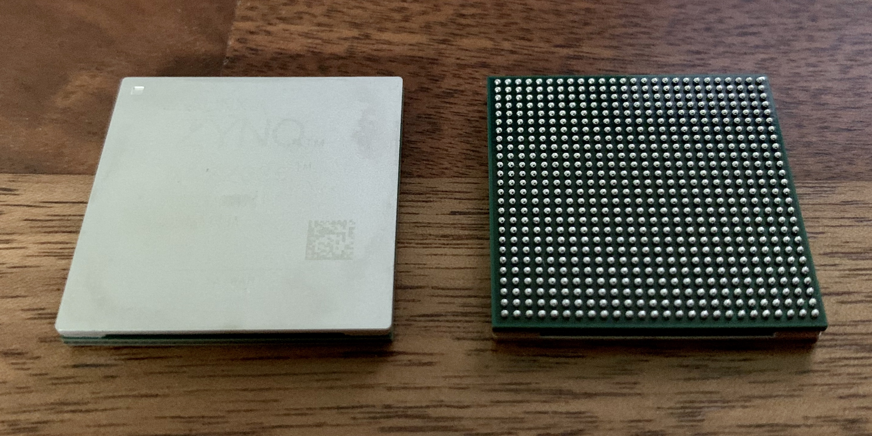
Things really started coming together when in March I found a vendor on eBay selling Xilinx Zynq XC7Z035 chips, refurbished, for the very reasonable price of $120. If you look on Digikey, these chips are normally really expensive in small quantities, like $1700 expensive. And they have reasons to be expensive, these are truly massive parts with dual ARM Cortex A9 CPU cores and 275k logic elements (that could fit multiple dozens of Gameboys, for reference).
The seller said they were “refurbished”, which I assumed meant they were removed from some PCB, cleaned up, and reballed. It’s actually quite common for parts sold on eBay from China. I heard someone joking at Supercon that “on Digikey you can buy parts on cut-tape or waffle-packs; from China you can order cut-PCB”. For expensive chips, a lot of the time you just buy a chunk of PCB with the chip you want on it!
With giant FPGAs in-hand, I couldn’t put off building the Gameslab anymore. Also, I needed to put together a board to see if these parts were legit before my eBay review period ended.
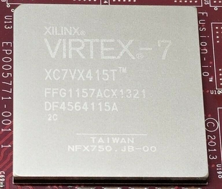 Notice what's around the big shiny FPGA part? It's still on a PCB!
What’s on that board?
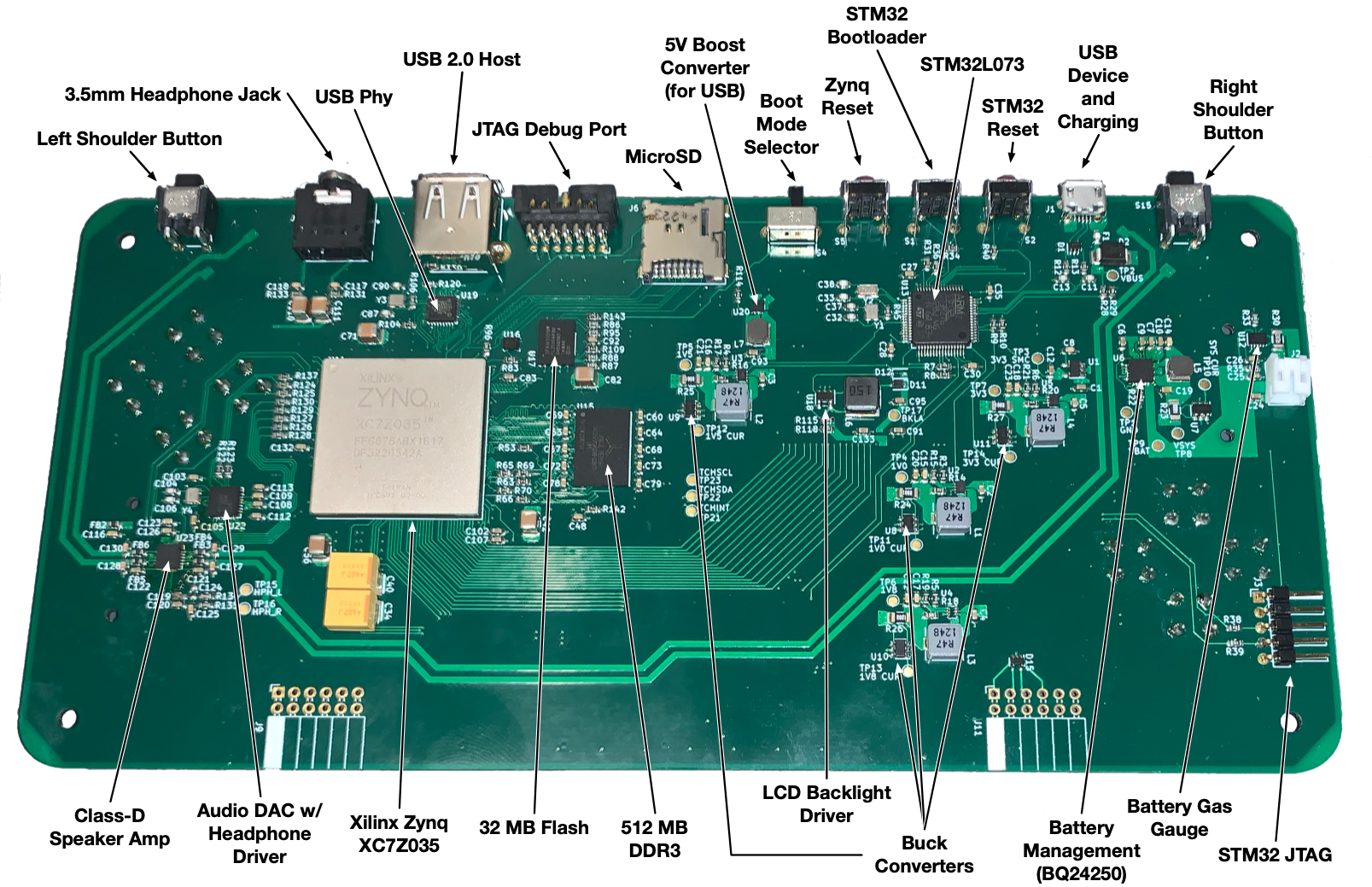
The Gameslab has about 360 parts on the bill of materials, making it the most complicated board I’ve ever designed. The board is roughly divided into a few subsystems:
Power
The Gameslab is powered by a Lithium polymer battery pack, charged via a USB micro jack. The USB jack can also power the system while running, thanks to the TI BQ24250 IC managing the battery. In the schematic below, you’ll also notice a STC3115 battery gas gauge on the low side of the battery (don’t copy this schematic for that… I haven’t tested it yet!). And, at the very top of the schematic, there’s a current sense amp for the main system rail that goes to all the other converters. I didn’t really know the power consumption to expect from this FPGA, since it also depends highly on what you configure in the fabric, so I put instrumentation on all of the voltage rails.
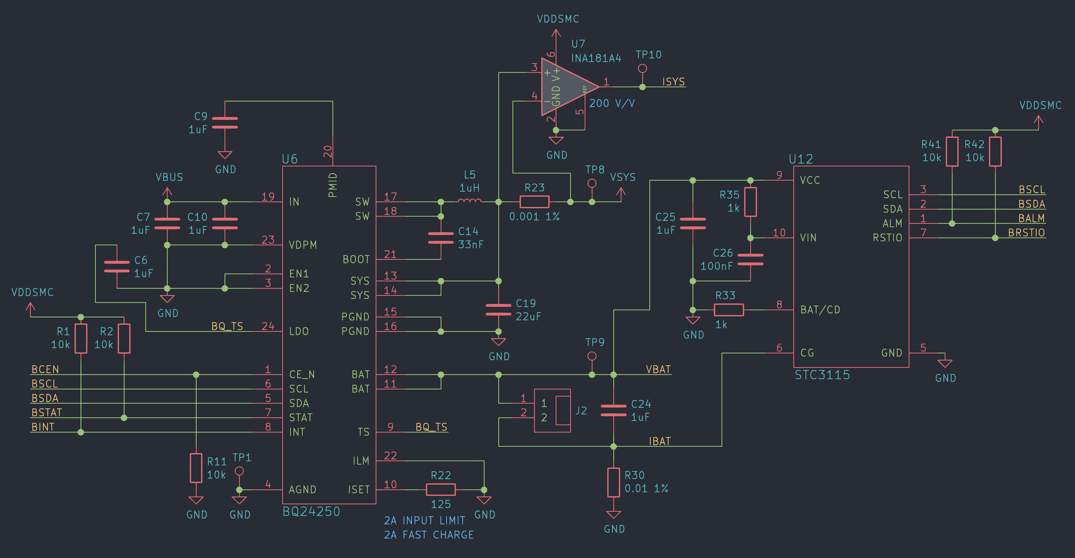 The awesome Solarized Dark color scheme comes from the kicad-color-schemes project
The rail from the BQ24250 drives an LDO to power the STM32L073 system supervisor, four individual switching regulators for the 1.0 V, 1.5 V, 1.8 V, and 3.3 V rails, the LCD backlight driver, and the 5 V USB boost converter. You can find these in the full schematic (warning: it’s a one-giant-semi-organized-sheet™ schematic).
The system supervisor, a STM32L073, manages the BQ24250 over I2C, measures the voltage and current on each rail, and is responsible for bringing up each rail to the FPGA in order, amongst other things. The STM32L0 series of microcontrollers are perfect for this application since they are low power, but still have a built-in USB peripheral for things like a TTY over USB.
Giant Zynq FPGA
The giant Zynq FPGA subsystem (GZF) contains the Zynq part with 512 MB of DDR3 DRAM. The DDR3 RAM can operate up to 533 MHz, giving a throughput up to 1066 Mbit/s per data line. Here, 16 data lines are used for a combined, theoretical bandwidth of ~2132 MB/s (not real-life bandwidth at all; 80-90% effiency is considered really good under varied loads).
The Zynq boots from a 32 MB quad SPI flash from Cypress, a S25FL256S. A Microchip USB3320C adds a USB 2.0 host port, and there’s a MicroSD slot (and it’s backwards… because of stupid, badly drawn datasheets). The Zynq is also connected to the system supervisor (STM32L073) by I2C and a UART, so the u-boot and Linux consoles can be dumped to USB.
Multi-touch screen
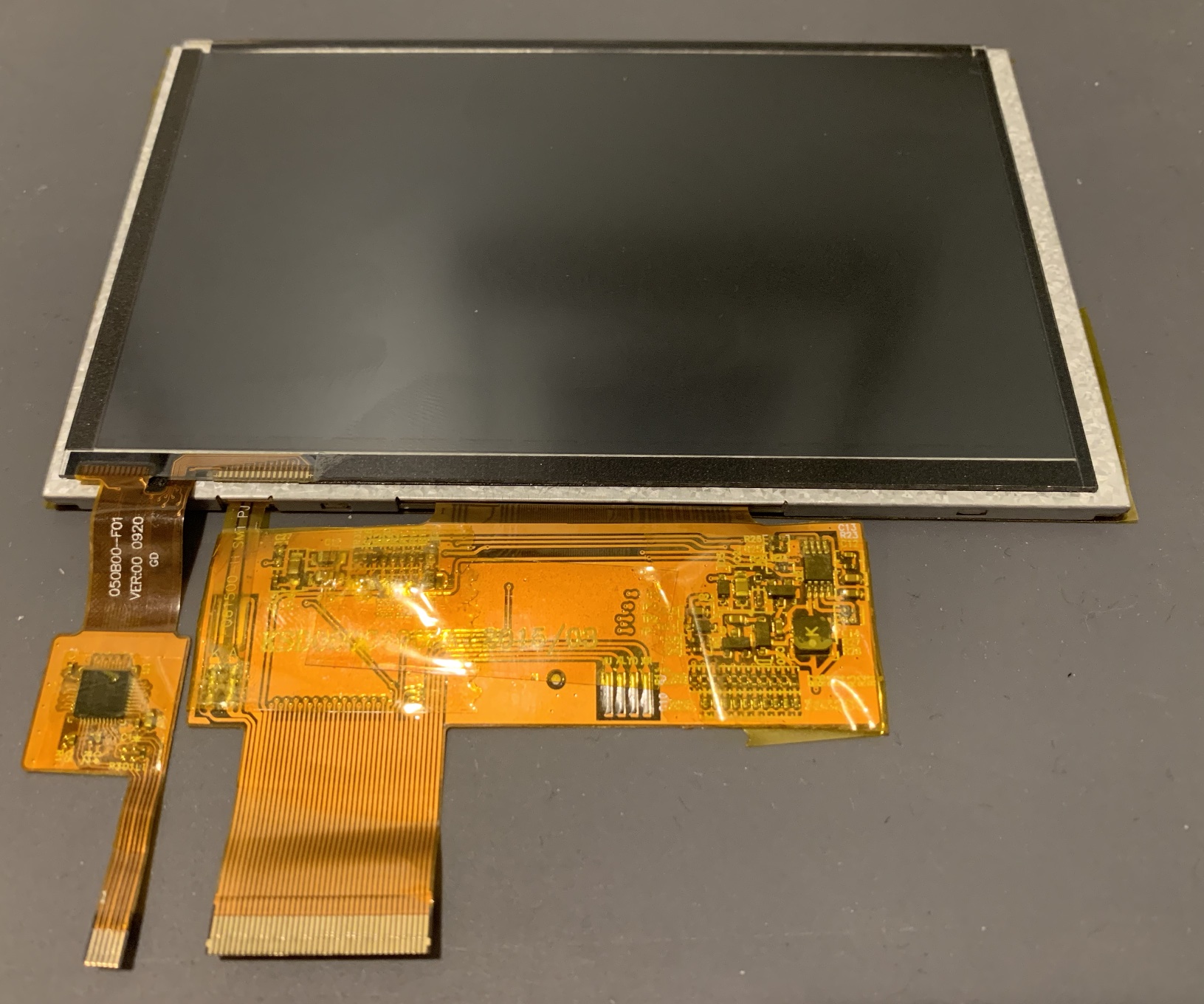
The screen on the Gameslab is a 5-inch 800x480 TFT display with a multi-touch panel over it. I found it on this website, and they will even attach the touchscreen for you with tiny double-sided tape. Be warned though, I wouldn’t buy the connectors they sell. I tried using those on a prototype board for the display, and they break pretty easily when you connected and disconnect the display repeatedly. Instead, I found some awesome connectors on Digikey that have a little lever that comes up, which is much easier to wiggle with my fat fingers.
Connecting the LCD to the FPGA is pretty simple, since it’s a giant parallel interface. There are 24 bits for color (RGB with 8 bits per channel), a vertical sync line, a horizontal sync line, and some enables. The LCD lines are driven directly from the FPGA I/O port at 3.3 V LVCMOS. The backlight is a little more complicated, since it needs a driver that generates boost voltage high enough to drive the whole chain of LEDs. Finally, the multi-touch interface is over I2C to the ARM Cortex A9 subsystem of the Zynq.
The Zynq doesn’t contain a LCD controller nor does it have any graphics accelerators at all. That all has to be implemented in the FPGA fabric, which is awesome!
Buttons and thumbsticks
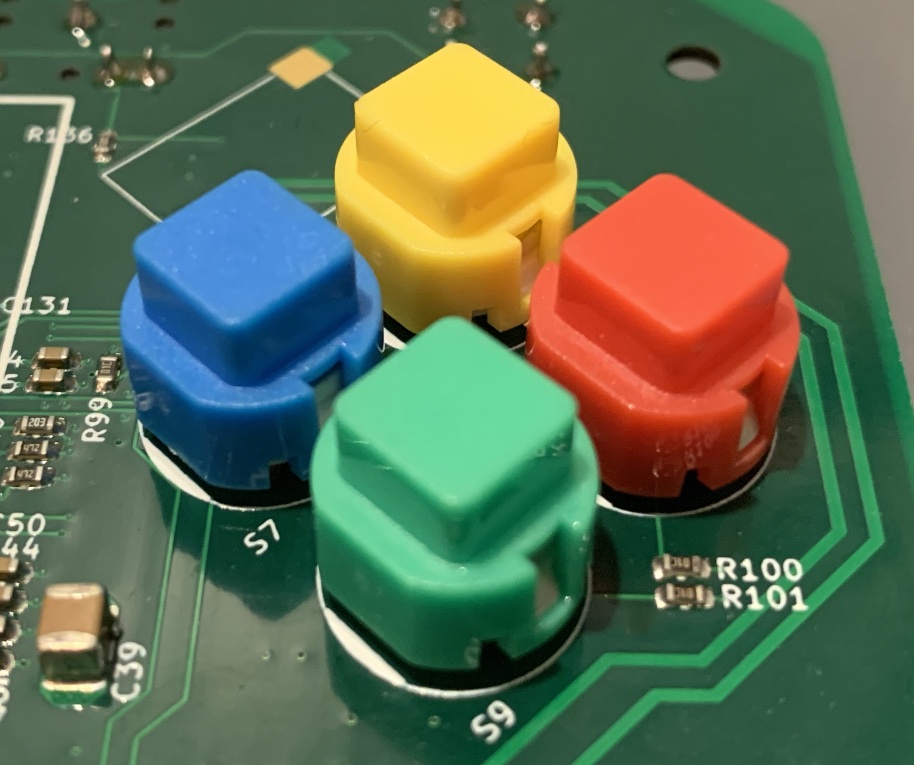
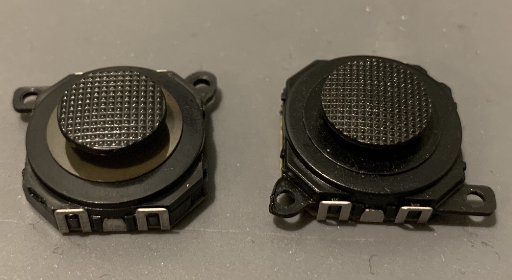
The Gameslab has 4 colored buttons on the right, 4 grey directional buttons on the left, left & right shoulder buttons, and two thumbsticks. The buttons are kind of wobbly on the PCB, but with the front panel over them, they feel great! Several people at Supercon asked me for the part number for these nice buttons, so here’s the datasheet. I bought the thumbsticks from Sparkfun a long time ago… and I wish I had looked for different ones. These have exposed pads on the bottom that are a royal pain to solder. Apparently there are similar thumbsticks out there with through-hole pins; that would’ve made my life so much easier!
Sound
The Gameslab’s sound subsystem is pretty simple: a stereo codec with a built-in headphone amp, and a class-D stereo amp to driver two speakers. Any fancy sound effects or mixing will be done in the FPGA fabric before going out over I2S to the codec. Thank you John Schuch (@JohnS_AZ) and Alex Schultz for helping me with the sound subsystem at our Hardware Happy Hour in Phoenix, and for letting me know that my class-D amp should probably have a filter on the output or things could get very bad.
Assembling this monster
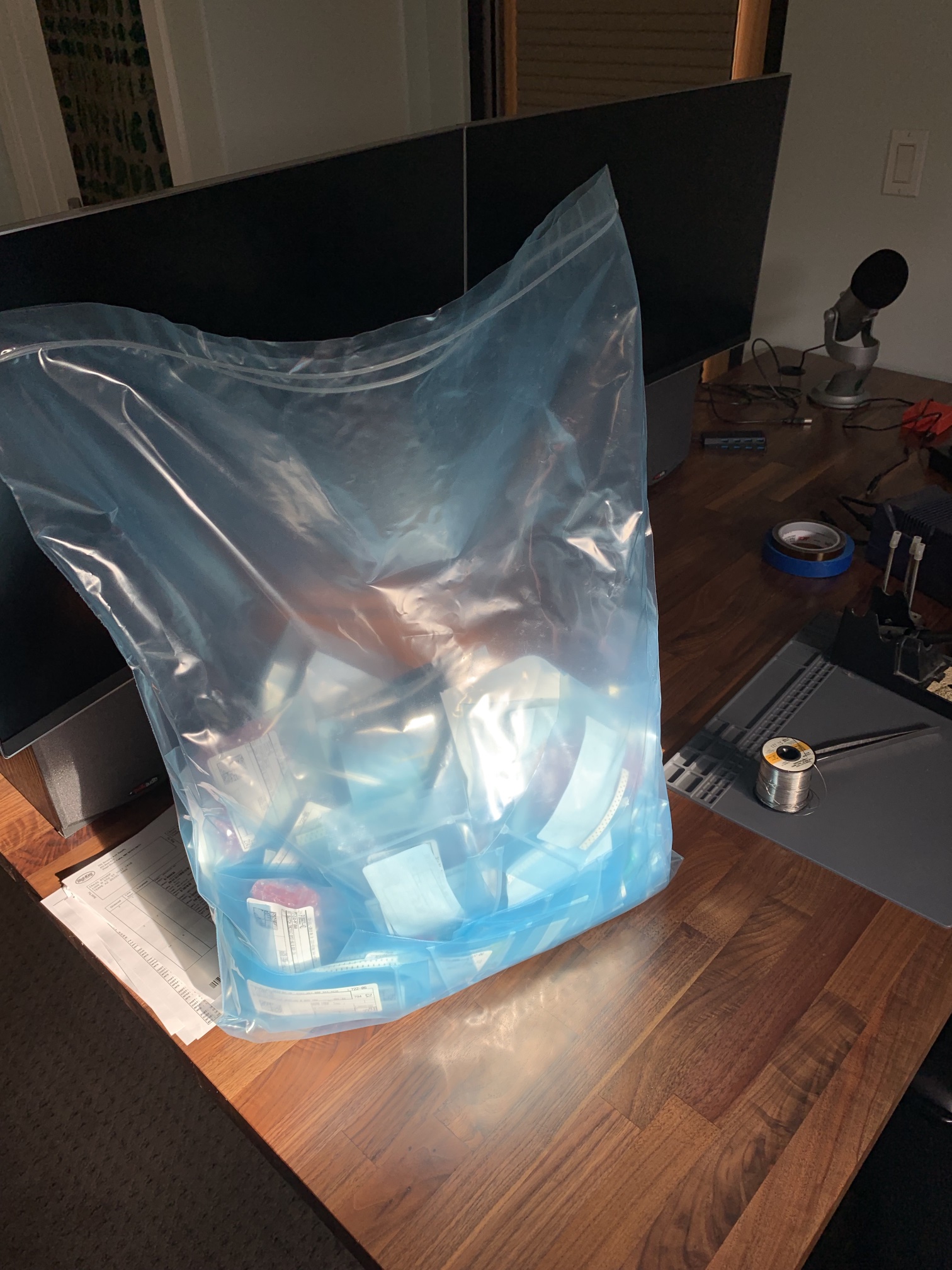
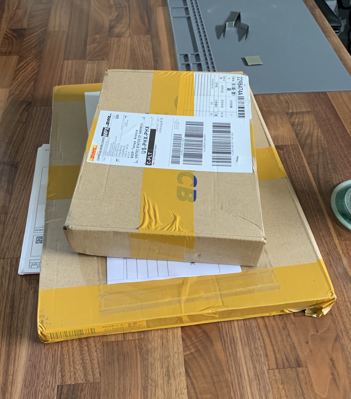
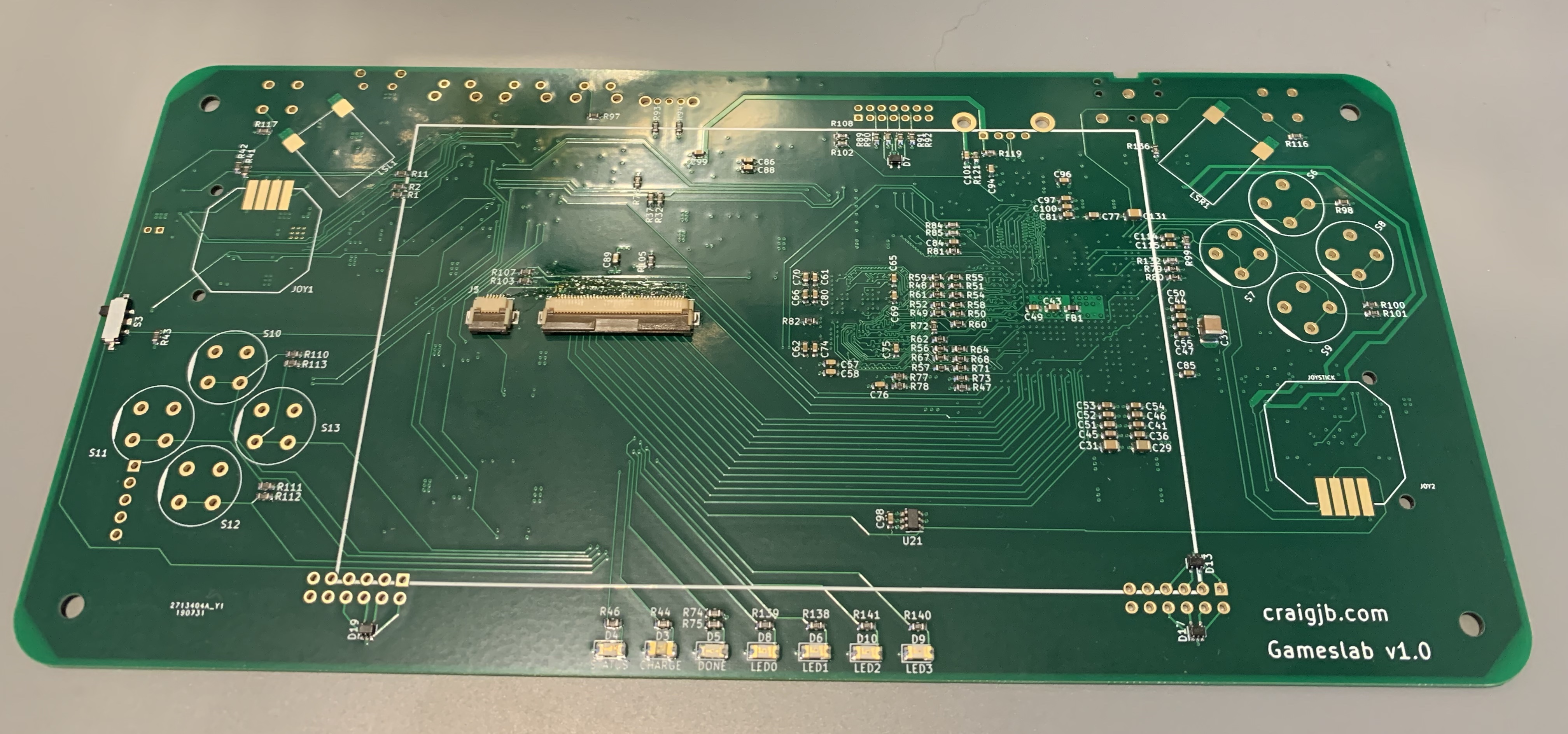
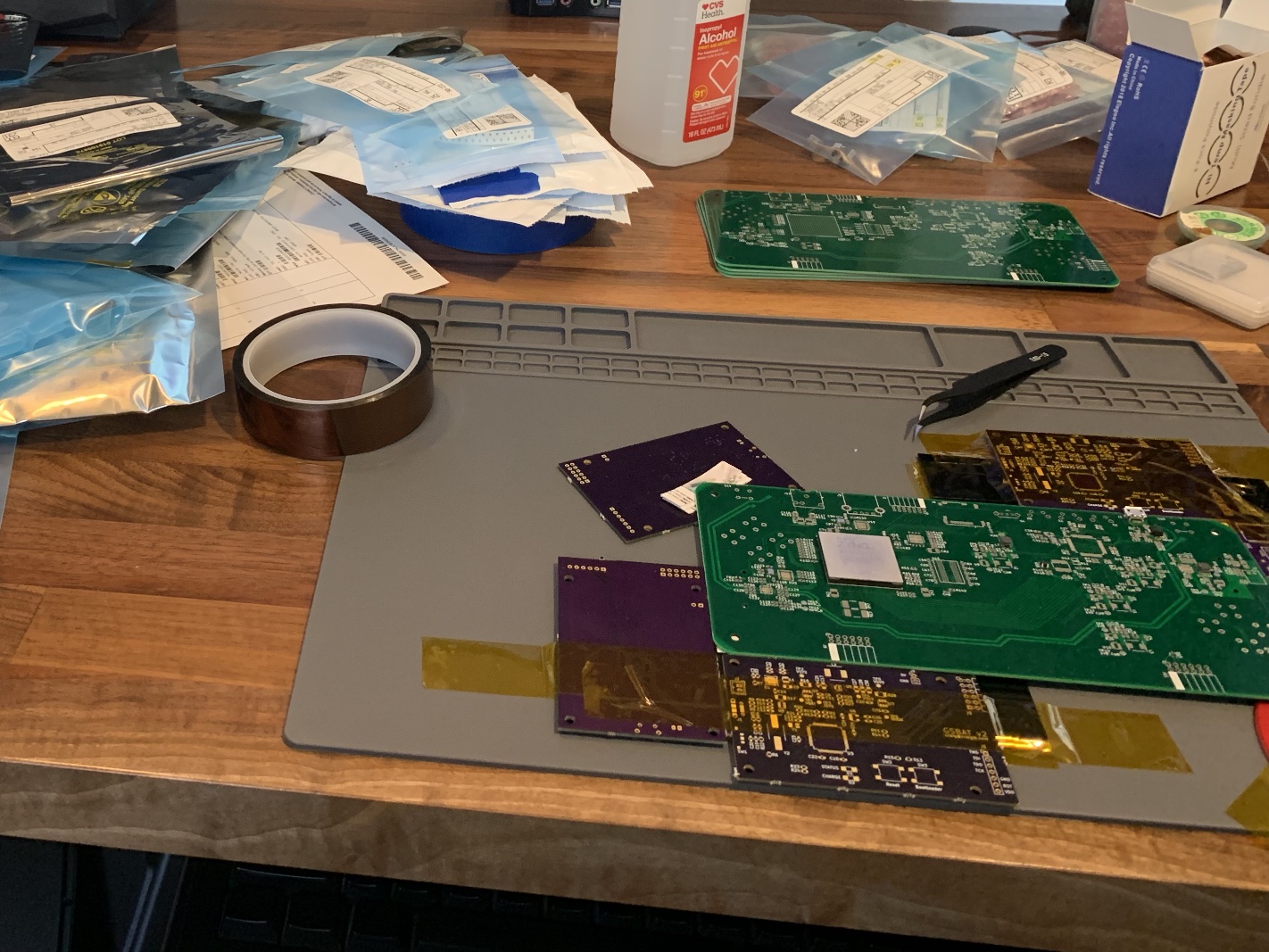
Assembling the Gameslab PCB was a long and patience-testing endeavor. It all starts with the biggest bag of Digikey parts I’ve ever received and the boxes from JLCPCB with the PCBs and stencils. JLCPCB sends you giant 380x280 mm stencils by default, and they are pretty big to work with (bottom box).
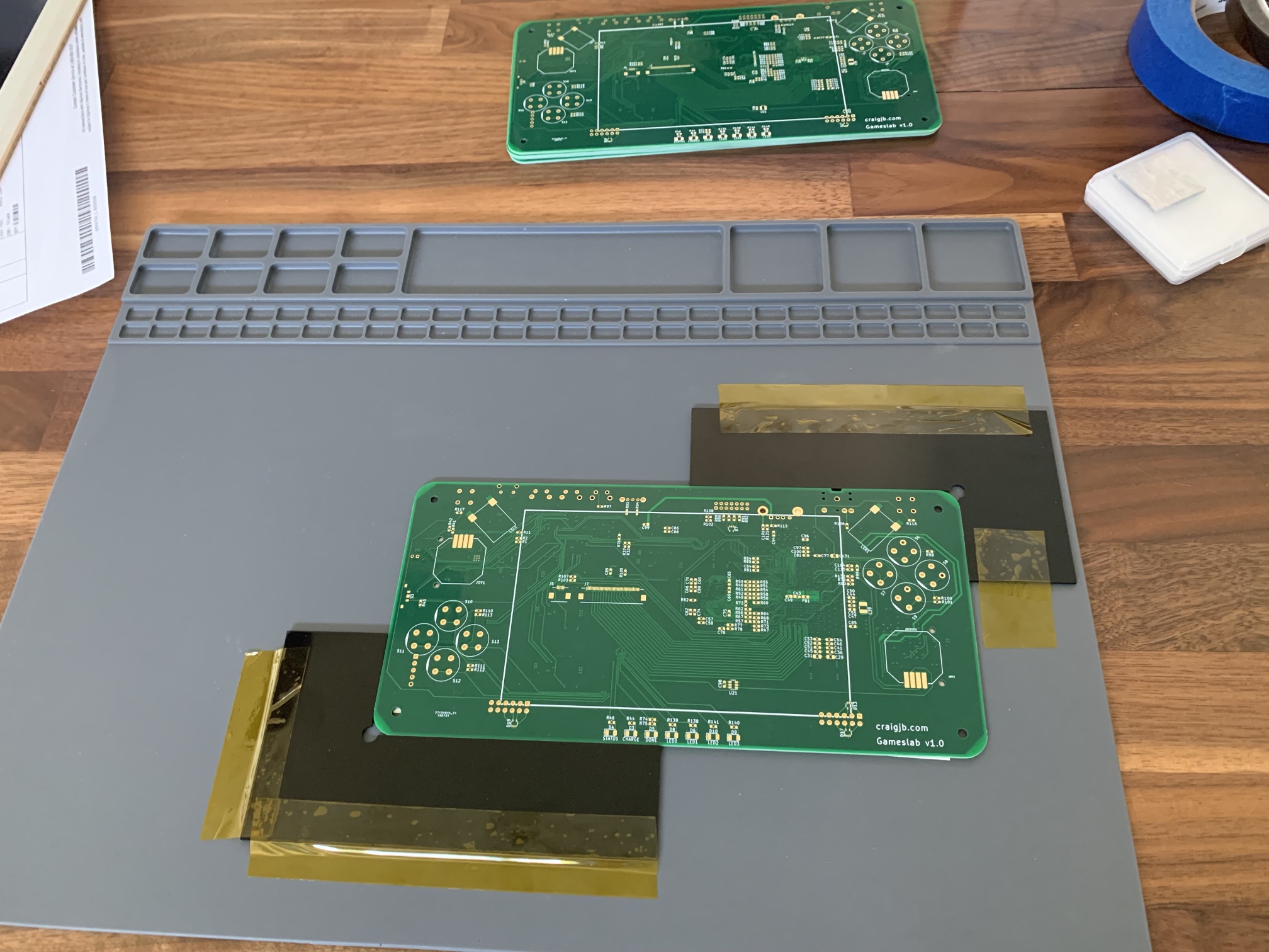
It’s absolutely critical to make sure the PCB is secured in place incredibly well. I use these two L-brackets and plenty of tape to make sure it doesn’t move at all. Nothing is worse than aligning the stencil perfectly, starting to apply paste, and then having the PCB shift underneath, ruining your hard work.
Applying solder paste to the board is pretty easy: squirt some out of the syringe onto the stencil and spread around with a applicator tool (the highly specialized tool is shown below).
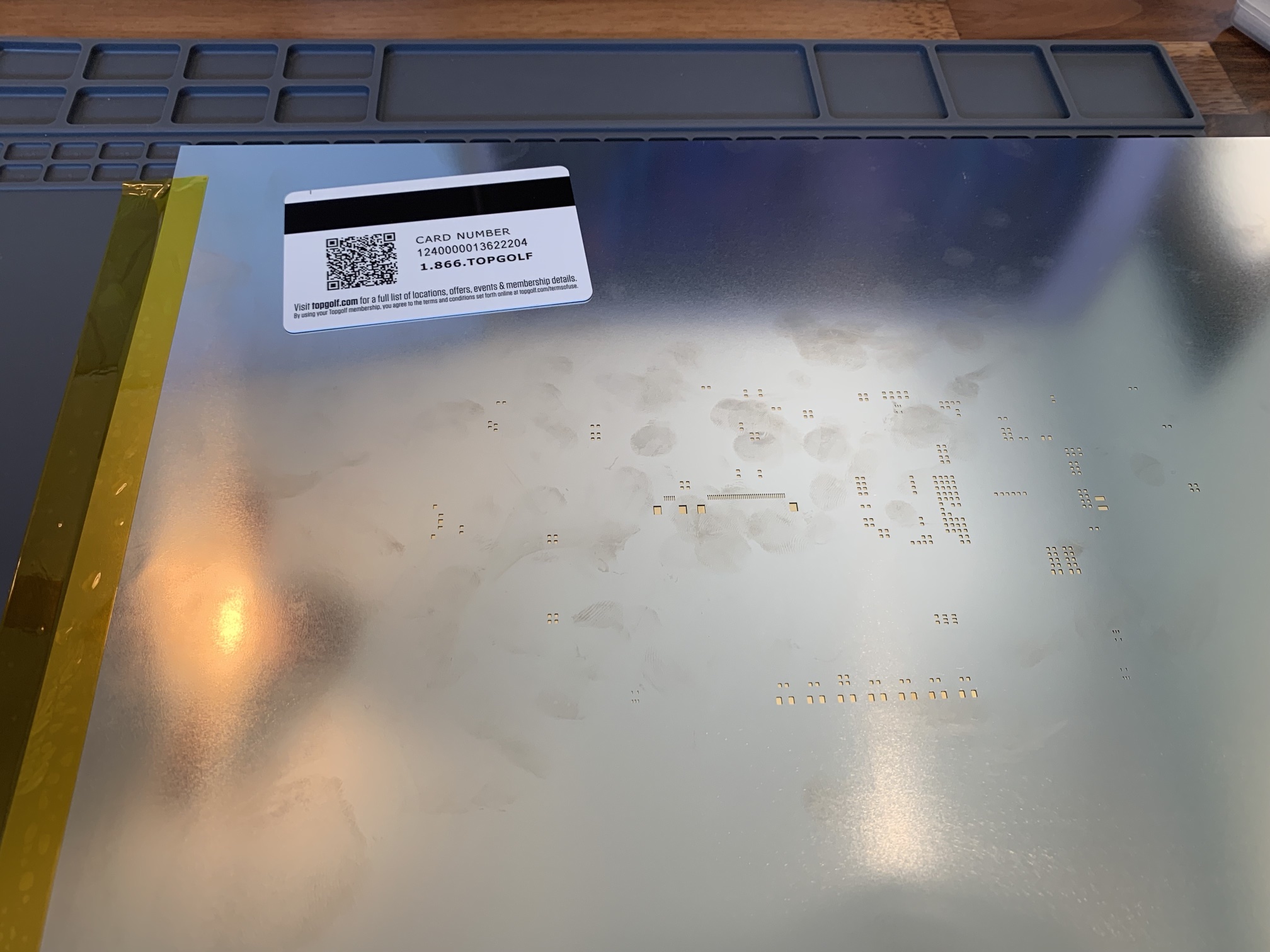 Don't steal my Top Golf membership that I only used once! Is that compromising information to have on the internet?
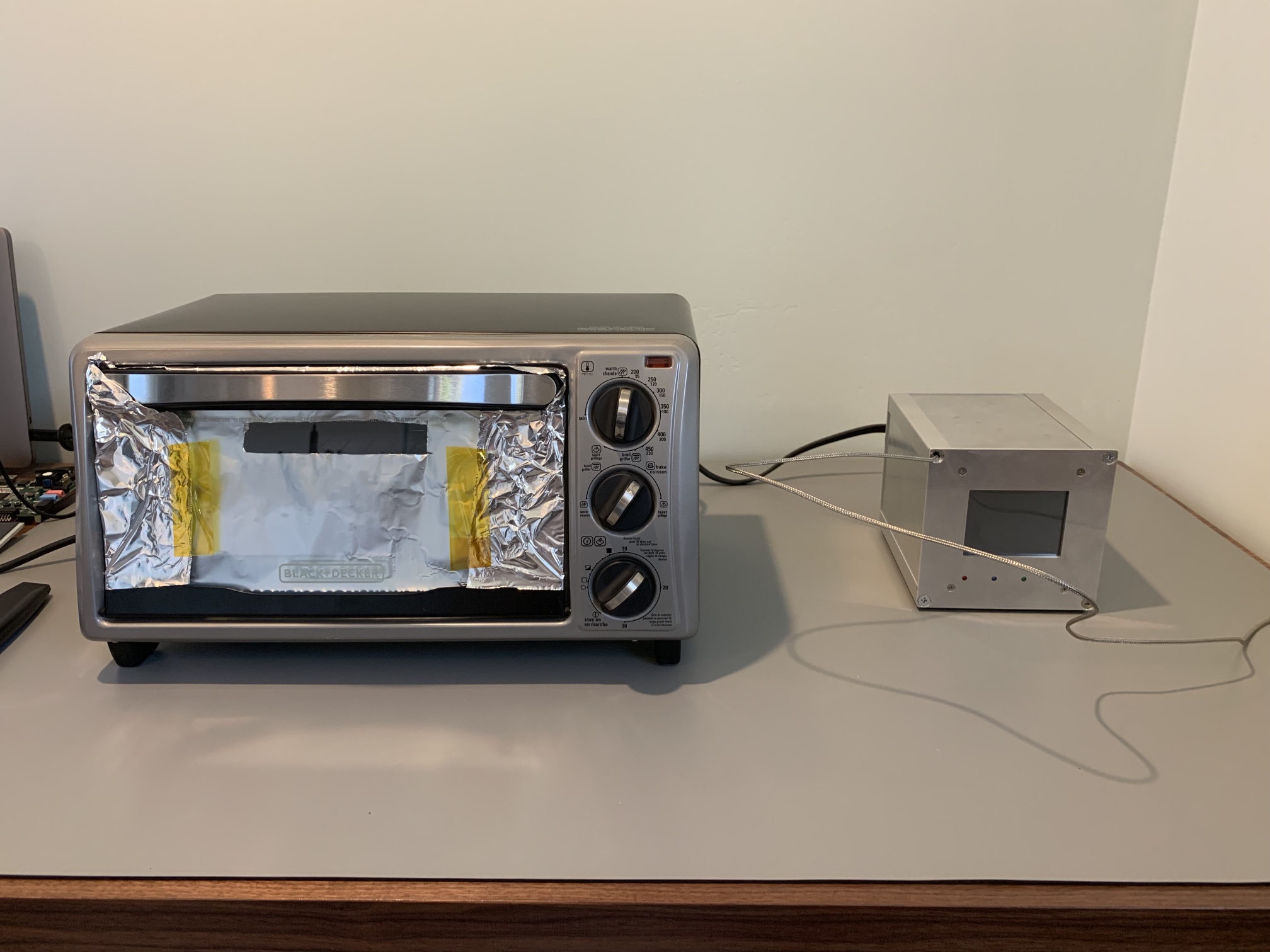
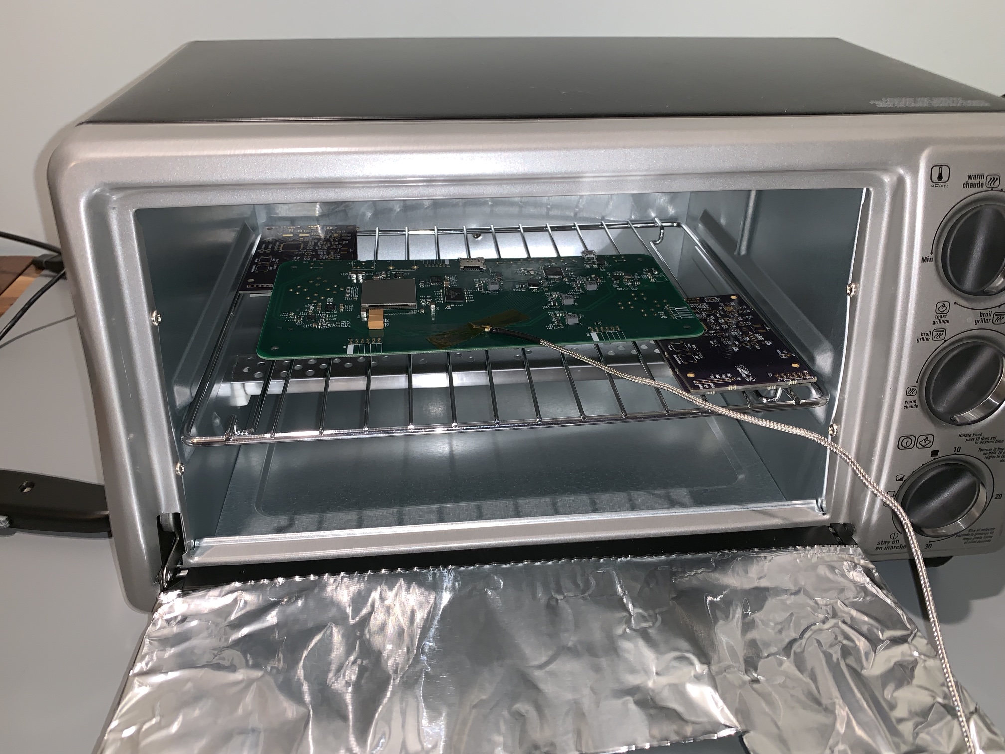
For the reflow, I use a top-of-the-line Black and Decker TO1313SBD 4-Slice toaster oven with EvenToast Technology. It’s specifically designed for even toasting of up to 4 slices of bread at a time, so it must be good for PCBs too. Oh, and next to it is a reflow oven controller I built from a kit awhile ago. It monitors the oven with a thermocouple and toggles the oven on-and-off with a PID control loop. You really don’t even need the controller for reflow, lots of people do it manually with a stopwatch and a multimeter temperature display, but I’m lazy.
After reflow, everything came out nicely, except a few bridges on the 0.5 mm pitch LCD connector. I touched those up quickly with some flux and an iron. I’m really starting to dislike 0.5 mm parts with gull-wing leads like this, or like TQFP parts. They always bridge on me. I haven’t had any problems with any of the QFN parts, so I think I’ll switch on future designs.
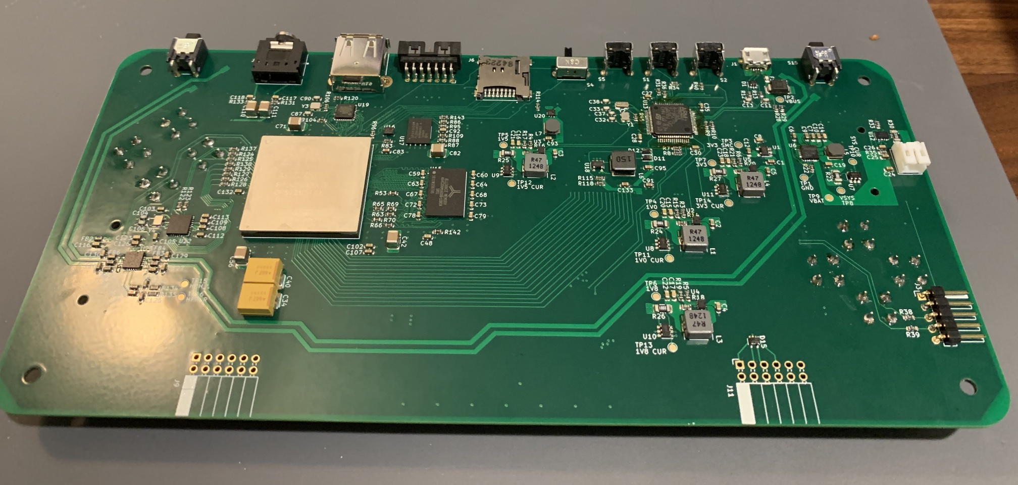
Stenciling the back side of the board turned out to be quite the challenge. Since the front side already has components on it, the board won’t lay flat. So, I had to put all kinds of things under it to hold up the edges, and I even had to stuff things under it to keep it stiff while spreading paste (notice all the scraps under the corners and edges in the picture). Placing the giant BGA part was actually one of the easiest, after I had the right tweezers. If you also have giant FPGAs to place, go on eBay and buy yourself some HOZAN P-848 Wide-Grip ESD-tip Tweezers.
Reflowing the back side of the board is a little more complicated since I wanted to prop up the board, just to make sure it didn’t shift around anything on the bottom. I had zero issues with parts on the bottom coming off, and they all survived the double reflow just fine. Solder surface tension is a powerful force. Although, I’m not quite sure it’d hold the giant FPGA on the back side.
Finally, after approximately six hours of stenciling, patient placement, reflowing, and through-hole soldering, the board is ready.
It boots!
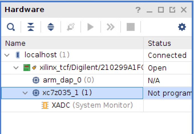
There actually was a bunch of work after assembling the board to troubleshoot a few things. First I had to debug why one of the rails wasn’t coming up. It turned out that one of the switching regulators had a bridged solder joint and needed a quick reflow with a hot-air gun. I’m never picking switching regulators in this tiny package again. Then, I figured out that my JTAG connector was actually backwards on the schematic and layout… luckily, it fit just fine flipped onto the other side. Once the JTAG connector was reversed, I was able to see the Zynq, and it showed the right part number!
I’m skipping a bunch of steps that I’ll write-up in more posts to come, like setting up the basic firmware on the STM32L073 in Rust (which also included creating a Rust device crate, a board-support crate, and porting a Rust USB device driver crate to the STM32L0). It also took awhile to get u-boot configured and ported, and then reconfigure my Linux device tree from my dev board prototype to boot Linux. But, the first time the Gameslab booted Linux was amazing!
More to come
I’ll definitely write a few more posts about Gameslab. I’m thinking the following, let me know what you think:
- More on the several iterations it took to get to the final working version
- Discussion about designing the case and having it manufactured
- Developing firmware for the STM32L0 with Rust and the RTFM RTOS
- Implementing the LCD controller in the FPGA fabric using SpinalHDL
- Bodging together a simple Linux driver for the LCD controller
- Setting up cross-compilation for Rust user-space games
- Creating custom graphics hardware in the FPGA fabric
- Using Linux device tree overlays to load new FPGA bitstreams and kernel modules on the fly
- Routing the DDR3 chip in KiCad
- Building a custom Debian root image

