
A large BGA, DDR3, & impedance control on a 6-layer PCB
A few months ago, I bought a couple Xilinx Zynq XC7Z035s off of eBay. These are beefy parts, even today! Each one has a dual core ARM Cortex A9, DDR controller + other peripherals, and a giant FPGA fabric (275k “logic cells”). The description did say “refurbished”, and hopefully that means just reballed, which isn’t uncommon for these expensive parts. Anyway, since I bought them, I’ve been itching to design a board for the parts and try them out. Specifically, I’ve wanted to get around to designing and building my Gameslab portable game console project. Well, after years of thinking about it, I finally put in the time to design the boards. And, in this post plus a few more to come, I’ll write about that process in detail. Today, I want to talk about how to even start, since these high-speed parts have more requirements on the PCB than your typical microcontroller.

PCB requirements
These are definitely the biggest BGA parts I’ve worked with to date, and the PCB design was proportionately more complicated. Even picking the number of layers to go for. If you look at most Zynq dev boards, they use something like 10 layers for routing out these chips. PCBShopper will give quotes for that, but the price is not so fun. Other hardware hackers have reflowed big BGAs on 4-layer boards from OSHPark, such as Andrew Zonenberg on his blog Silicon Exposed.
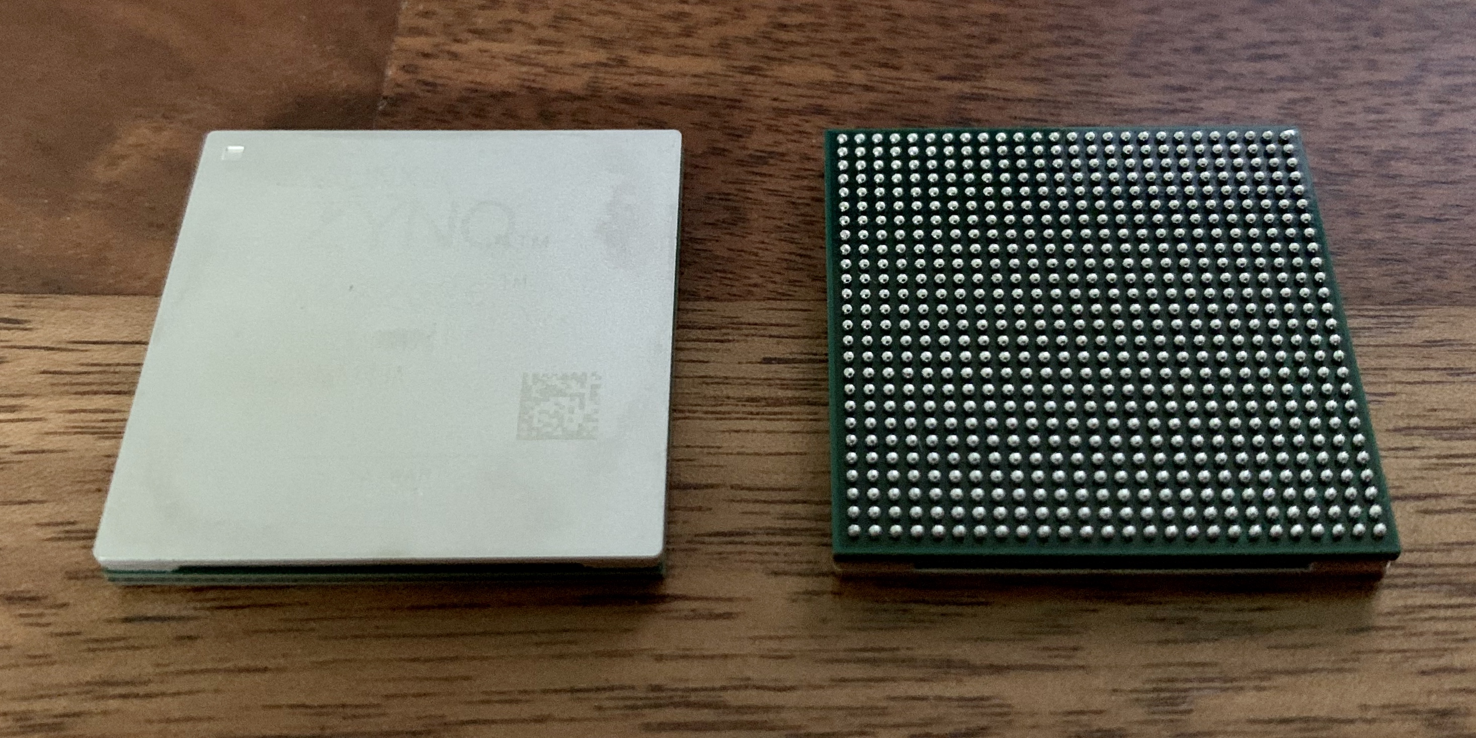
I thought about trying to use four layers, but routing the 16-bit DDR3 data bus with impedance matching would be super tight. I’m not using all the pins of the FPGA, in fact not even half of the IOs, so a 10 layer board definitely wasn’t necessary. It turns out, that the minimum line/space and total via diameter were the truly decisive factors. The Zynq BGA is a 1mm pitch part, and I only used through-vias, so a trace had to fit between the land pads. The DDR3 BGA is a 0.8mm pitch, but with vastly fewer IOs–also the standard DDR3 footprints have lots of room. So it should be ok.
Cost
If you take a look on PCBShopper, 6-layer PCBs boards are still pricey. I plugged in my estimated form-factor, picked 6 layers, selected 5 mil traces (my estimate), picked ENIG finished (definitely want ENIG for BGAs), and checked out the results. It wasn’t even a competition. JLCPCB estimated $158 for five pieces. The next estimate was from PCBWay at ~$300. I don’t have any favorites here, but with that pricing I could do two iterations for the price of one, and I definitely expected to iterate.
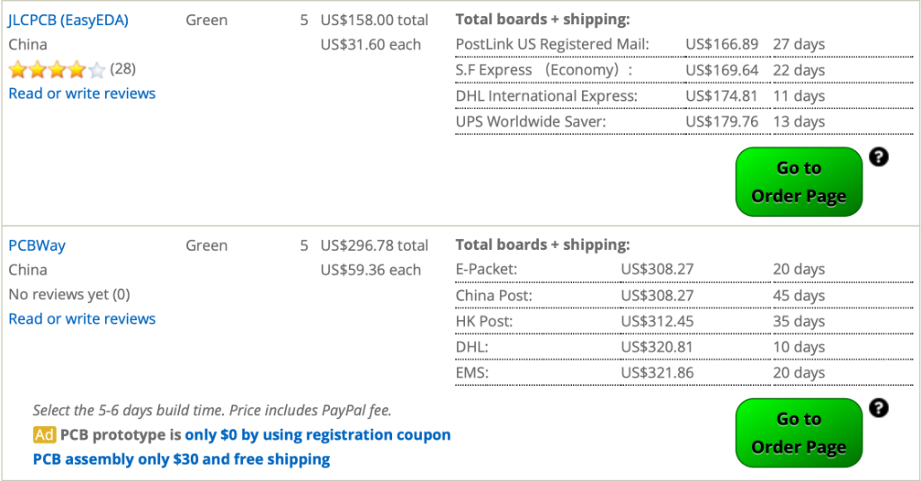
That pricing is insanely good. And, I knew that if this project worked on their 6-layer boards, it would open up a lot of other fun possibilities for future projects at a reasonable cost. If you pull up their capabilities page, they claim down to 3.5 mil traces. But, beware, they say that via to trace clearance must be 5 mil, even if trace to trace is 3.5 mil. Some EDA tools (cough KiCad) don’t have support for that. Also, their minimum total via diameter is 0.45mm (0.2mm drill with 125µm annular ring) which is a little big, but should be ok. The Zynq BGA pitch is 1mm, and 1.0 - 0.45 - 0.127 - 0.127 = 0.296mm (pitch - via size - spacing - spacing). So, it fits a trace between, no problem.
Stackups and impedance control
DDR3 runs at a high enough frequency, up to 533 MHz in this case (for 1066 Mbits/s per data pin), that we care about signal integrity. For DDR3, we care about impedance matching to prevent reflections that can cause glitches on the command or data bits, and we care about delay matching to ensure that the data bits or commmand bits all arrive at the chip before they are latched.
When designing a PCB, your main weapon against signal integrity problems is your stackup. The stackup defines what layers are in your PCB, what thickness each layer of copper is, and what the thicknesses of the cores or substrates between the copper layers are. The impedance of a uniform trace on any given layer can then be estimated from the trace width and the stackup dimensions. So, this makes planning your stackup very important, since not all stackups can give the impedance you need at a given trace width.
For example, here’s the 1.2mm thick stackup I used for the Gameslab board. It’s an “impedance-controlled” stackup, which means that the board house guarantees the thicknesses of the layers to within a certain tolerance (i.e. they throw out the ones outside of the tolerance).
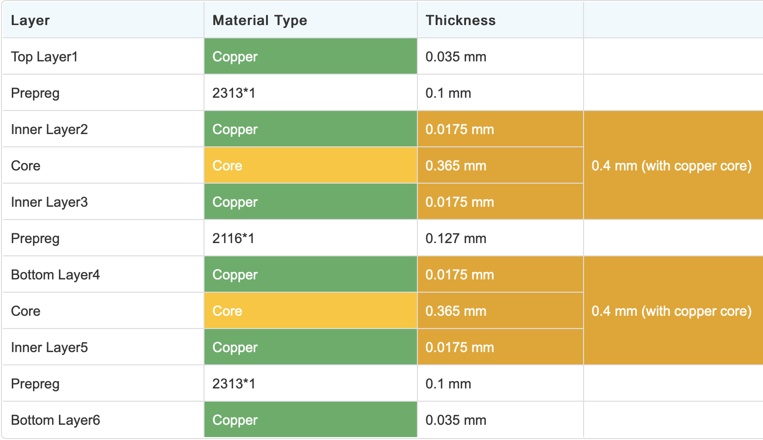 The JLCPCB 6-layer stackup for a 1.2mm thick impedance-controlled board
You can then use a stripline or microstrip impedance calculator to estimate your line impedance. Be warned though! The calculators only give you estimates, your board has tolerances (maybe 10%), your traces have width and spacing tolerances, and the formulas in the calculators are only approximations. So, it’s best to keep some margin in your design. In this case, since I only have one DDR3 part on the board, and all the traces are simple point-to-point connections, there’s plenty of margin. However, you can imagine if you’re desinging with multiple chips or a giant DIMM connector, there are impedance discontinuities all over the place.
I wanted to try to keep the DDR3 traces somewhere about 5 mils to escape the Zynq BGA, so I played around with the JLCPCB calculator until I landed on this:
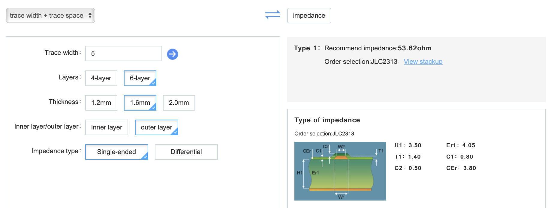
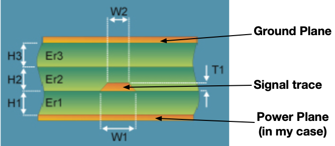
That’s for the outer traces, and looks pretty good. But, routing the DDR3 chip is much easier with three routing layers, so I also played around with the calculator to figure out the stripline impedance on the internal layers. Here, it’s important to mention that the copper layers on either side of your trace are incredibly important to the impedance as well. Typically, for a microstrip on an outer layer, the copper below is a ground plane, and called the “reference plane”. For internal traces, you have to consider the copper above and below. Technically, your reference plane does not have to be a ground plane either, and in the Gameslab design I used the DDR3 power plane as one of the reference planes for the internal routing layer. For a high-frequency AC signal, the DC voltage on the power plane looks like a ground plane too.
Technically, the DDR3 controller on the Zynq specifies that the traces should be routed at 40 ohms, but going to 40 ohms on this design would result in some pretty big traces and make routing complicated. Since the design only has one chip in the point-to-point configuration, I thought that 50 ohm would cut it. Also, since the design only has one chip, I could place it as close as possible to the Zynq part to minimize the total trace lengths. At 533 Mhz, a wavelength is approximately 300mm on a PCB (rough estimate), and at 1/10 of the wavelength, reflection problems are much less of a concern. So, if my traces are approximately 30 mm in length or less, the design should have good enough margin to work if I match the delays (we’ll see how robustly).
That’s enough talk about stackups and impedance. I’ll write about actually routing this thing another time, and how to match the trace delays (not lengths!) in KiCad, including the Excel-fu I used to calculate the delays for different layer signal velocities and how to workaround series termination resistors in KiCad.