
FPGA Game Boy Part 3: ALU and some microcode
In the last post, I showed the test bench that loads an assembled Game Boy binary program, and we looked at the waveform output showing that the instruction fetch cycle worked. However, the instruction itself didn’t do anything. This time, I’m going to work on implementing the basic register-to-register arithmetic instructions, which are some of the simplest out of the whole instruction set. First, the CPU needs an ALU before it can execute arithmetic instructions. Then, it needs an instruction decoder to turn the op codes into the right control signals.
The ALU
If we look again at the CPU architecture diagram from a couple posts ago, one operand to the ALU comes from a temp register, and the other always comes from the accumulator, hence the name accumulator. The ALU result is produced combinatorially and stored into one of the multiplexed registers. A set of four flags (zero, add/subtract, half-carry, carry) are also output and used to update the F (or flags) register. Not all ALU operations update all flag bits.
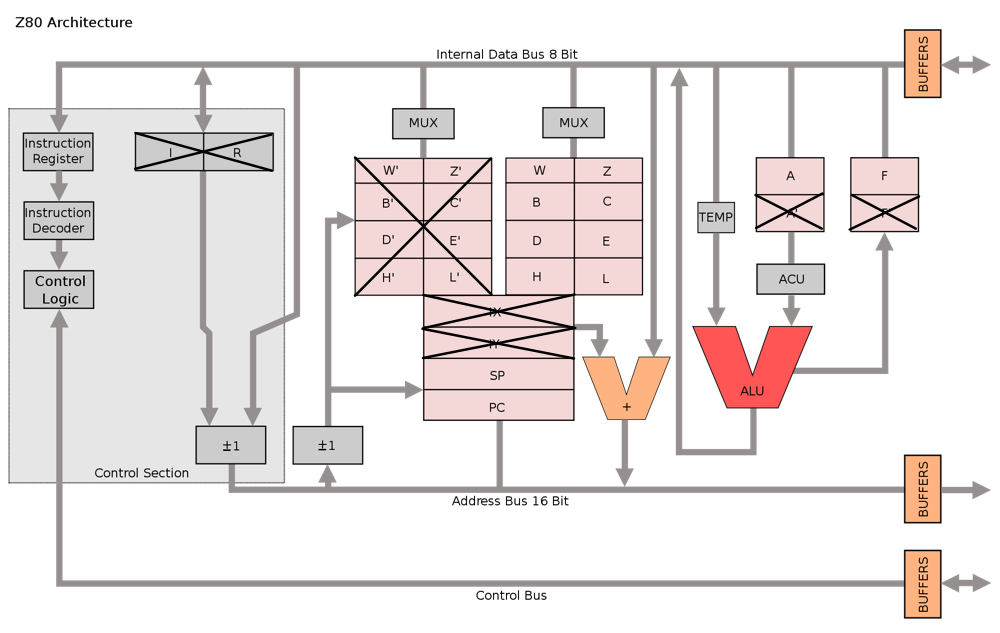 From Spencer Steers's Game Boy Development Book, with some edits.
You might have noticed that I forgot the A (accumulator) and F (flags) registers in the previous post. I updated the definitions to fix that; the new indices are shown below. I didn’t include an index for 16-bit AF, since the accumulator and flags register aren’t accessed together as a 16-bit value.
  object Reg16 {
    val WZ = 1
    val BC = 2
    val DE = 3
    val HL = 4
    val SP = 5
    val PC = 6
  }

  object Reg8 {
    val A = 0; val F = 1
    val W = 2; val Z = 3
    val B = 4; val C = 5
    val D = 6; val E = 7
    val H = 8; val L = 9
    val SPH = 10; val SPL = 11
    val PCL = 12; val PCH = 13

    // auto calculate bits needed to represent register index
    def DataType = UInt(log2Up(PCH) bits)
  }
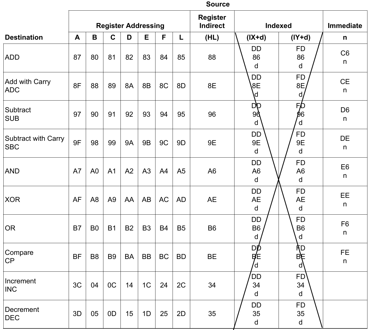
To get a list of ALU operations that we need to implement, I searched through the Z80 manual and found the chart below on page 50. You’ll notice I crossed out some instructions, and that’s because the Game Boy LR35902 doesn’t have the Z80’s IX and IY registers, nor the instructions that use them. To keep things simple, we’ll start with the Register Addressing variants, since they execute in a single M-Cycle (four T-Cycles) and don’t require memory reads other than the op code fetch.
Let’s go ahead and list out the possible ALU operations using a SpinalHDL enum. I’ll also list out the flag register bits.
object Cpu {

  ...

  object AluOp extends SpinalEnum {
    val Nop, Add, Adc, Sub, Sbc, And, Xor, Or, Cp, Inc, Dec = newElement()
  }

  object Flags {
    val C = 4
    val H = 5
    val N = 6
    val Z = 7
  }
}
Then, we’ll start by defining the ALU’s IO, and some helpers for implementing the internal operation. Since the ALU has to output a carry flag, it’s easiest just to use an extra bit internally. Then, for the 8-bit output the 9th bit is chopped off, but it shows up in the flags if that operation updates the carry flag. The Z80 also has a half carry flag bit. I don’t quite know yet what it’s used for in the Game Boy, since the LR35902 doesn’t have any branch instructions with a half-carry condition. But, we’ll go ahead and implement it anyway.
class CpuAlu extends Component {
  import Cpu._

  val io = new Bundle {
    val op = in(AluOp())
    val flagsIn = in UInt(8 bits)
    val flagsOut = out UInts(8 bits)
    val operandA = in UInt(8 bits)
    val operandB = in UInt(8 bits)
    val result = out UInt(8 bits)
  }

  // use 9-bits internally so the carry bit is easily available
  val wideResult = UInt(9 bits)
  io.result := wideResult(7 downto 0)
  val wideOpA = io.operandA.resize(9 bits)
  val wideOpB = io.operandB.resize(9 bits)

  // grab carry bits
  val carry = wideResult(8)
  // Z80 has half-carry and half-borrow bits as well
  val halfCarry = (
    wideResult.asBits(4) &&
    wideResult.asBits(3 downto 0) === B(0, 4 bits)
  )
  val halfBorrow = (
    !wideResult.asBits(4) &&
    wideResult.asBits(3 downto 0) === B(0xF, 4 bits)
  )

  // by default, pass flags through
  io.flagsOut := io.flagsIn
}
Now, to make setting the flags for all the different operations a little bit more succinct, I’ll make a quick helper function for updating the flags.
  // helper for optionally setting or resetting flags
  def setFlags(c: Bool, h: Bool, n: Bool) = {
    io.flagsOut(Cpu.Flags.C) := c
    io.flagsOut(Cpu.Flags.H) := h
    io.flagsOut(Cpu.Flags.N) := n
    io.flagsOut(Cpu.Flags.Z) := (wideResult(7 downto 0) === 0)
  }
And now, let’s add a switch statement to handle the different ALU operations. This instruction set chart is handy for looking up which flag bits are updated by the different operations. The only tricky thing to notice is that the subtraction instructions use the carry bits as borrow bits. For the full borrow bit, it’s just carry bit inverted; however, half-borrow is calculated separately in the above snippets. Other than that, the ALU is straightforward.
  switch(io.op) {
    is(AluOp.Nop) {
      wideResult := wideOpB
    }
    is(AluOp.Add) {
      wideResult := wideOpA + wideOpB
      setFlags(carry, halfCarry, False)
    }
    is(AluOp.Adc) {
      wideResult := wideOpA + wideOpB + io.flagsIn(Cpu.Flags.C).asUInt
      setFlags(carry, halfCarry, False)
    }
    is(AluOp.Sub) {
      wideResult := wideOpA - wideOpB
      setFlags(carry, halfBorrow, True)
    }
    is(AluOp.Sbc) {
      wideResult := wideOpA - wideOpB - io.flagsIn(Cpu.Flags.C).asUInt
      setFlags(carry, halfBorrow, True)
    }
    is(AluOp.And) {
      wideResult := wideOpA & wideOpB
      setFlags(False, True, False)
    }
    is(AluOp.Xor) {
      wideResult := wideOpA ^ wideOpB
      setFlags(False, False, False)
    }
    is(AluOp.Or) {
      wideResult := wideOpA | wideOpB
      setFlags(False, False, False)
    }
    is(AluOp.Cp) {
      wideResult := wideOpA - wideOpB
      setFlags(!carry, !halfCarry, True)
    }
    is(AluOp.Inc) {
      wideResult := wideOpB + 1
      setFlags(io.flagsIn(Cpu.Flags.C), halfCarry, False)
    }
    is(AluOp.Dec) {
      wideResult := wideOpB - 1
      setFlags(io.flagsIn(Cpu.Flags.C), halfBorrow, True)
    }
  }
The decoder
Before we can hook up the ALU and run some instructions, we’re going to need an instruction decoder to generate some of the control signals. For now, it’s going to control which ALU operation to perform, what operands to use, and where to store the results. However, going forward it will also control memory reads, memory writes, and more. To organize all of the different control signals for each M-Cycle for each instruction, I want to try a microcode-like approach. We don’t really need to be able to update the microcoded instructions, like a true RAM or ROM+RAM microcode implementation; however, I would like to have all of the instruction op codes and their control signal definitions in one place.
So, to get started, I’ve defined the control signals we know about so far, and added the microcode for the nop and inc a instructions. I also used a bit of Scala functional magic to calculate how big the register for tracking the current M-Cycle should be based on the microcode contents. This way, adding new instructions that have more M-Cycles doesn’t require editing definitions elsewhere. This is one of the main reasons I’m enjoying SpinalHDL so much. In Verilog, I’d make changes and constantly forget to update other affected defintions. And, since Verilog has a weak type system, it didn’t complain half the time, which means I wasted a ton of time in the simulator tracking down simple bugs.
object CpuDecoder {
  import Cpu._

  case class MCycle(
    aluOp: SpinalEnumElement[AluOp.type],
    opBSelect: Option[Int],
    storeSelect: Option[Int]
  )

  val Microcode = Seq(
    // nop
    (0x00, Seq(MCycle(AluOp.Nop, None, None))),
    // inc a
    (0x3C, Seq(MCycle(AluOp.Inc, Some(Reg8.A), Some(Reg8.A))))
  )

  val DefaultCycle = Microcode(0)._2(0)

  val MaxMCycles = Microcode.map(code => code._2.length).reduceLeft(_ max _ )
  def MCycleDataType = UInt(log2Up(MaxMCycles) bits)
}
Next, inside the component class, I’ll just decode each cycle out of the microcode and set the control signals accordingly. I added a couple of extra signals to the IO, loadOpB and store, that indicate whether operand B should be loaded into the temp register and whether the output of the ALU should be stored back into the register file. Some ALU ops, like nop, should not affect the temp register or register file since they’ll be used as part of more complicated instructions like memory loads and writes.
class CpuDecoder extends Component {
  import Cpu._
  import CpuDecoder._

  val io = new Bundle {
    val mCycle = in(MCycleDataType)
    val nextMCycle = out(MCycleDataType)
    val ir = in UInt(8 bits)
    val aluOp = out(AluOp())
    val opBSelect = out(Reg8.DataType)
    val loadOpB = out Bool
    val storeSelect = out(Reg8.DataType)
    val store = out Bool
  }

  def decodeCycle(cycle: MCycle) = {
    io.aluOp := cycle.aluOp
    cycle.opBSelect match {
      case Some(x) => {
        io.opBSelect := x
        io.loadOpB := True
      }
      case None => {
        io.opBSelect := 0
        io.loadOpB := False
      }
    }
    cycle.storeSelect match {
      case Some(x) => {
        io.storeSelect := x
        io.store := True
      }
      case None => {
        io.storeSelect := 0
        io.store := False
      }
    }
  }

  // default to NOP
  decodeCycle(DefaultCycle)

  // decode microcode instructions
  for(icode <- Microcode) {
    when(io.ir === icode._1) {
      for((cycle, i) <- icode._2.zipWithIndex) {
        when(io.mCycle === i) {
          decodeCycle(cycle)
          if(i == icode._2.length - 1) {
            io.nextMCycle := 0
          } else {
            io.nextMCycle := io.mCycle + 1
          }
        }
      }
    }
  }
}
Wiring it all up
Finally, we can wire up the new decoder and ALU components to execute some instructions. First, I’ll define the temp register that I missed before, and add a register for tracking the current M-Cycle. Then I’ll use those to wire up the decoder and ALU.
  val temp = Reg(UInt(8 bits)) init(0)

  val mCycle = Reg(CpuDecoder.MCycleDataType) init(0)

  val decoder = new CpuDecoder
  decoder.io.mCycle := mCycle
  decoder.io.ir := ir

  val alu = new CpuAlu
  alu.io.op := decoder.io.aluOp
  alu.io.flagsIn := registers8(Reg8.F)
  alu.io.operandA := registers8(Reg8.A)
  alu.io.operandB := temp
The T-Cycle state machine needs a few adjustments to use the new control signals as well. While reading the Z80 manual, I noticed they start M-Cycles with T1 instead of T0, so I adjusted the state naming to match. I also moved the address load and mreq assertion to t1State so that the data bus can be loaded into the temp register in t3State, before the ALU op in t4State.
  val tCycleFsm = new StateMachine {
    val t1State: State = new State with EntryPoint {
      onEntry {
        address := registers16(Reg16.PC)
        mreq := True
      }
      whenIsActive {
        mreq := False
        goto(t2State)
      }
    }
    val t2State = new State {
      whenIsActive {
        ir := io.dataIn
        registers16(Reg16.PC) := registers16(Reg16.PC) + 1
        goto(t3State)
      }
    }
    val t3State = new State {
      whenIsActive {
        when(decoder.io.loadOpB) {
          temp := registers8(decoder.io.opBSelect)
        }
        goto(t4State)
      }
    }
    val t4State = new State {
      whenIsActive {
        when(decoder.io.store) {
          registers8(decoder.io.storeSelect) := alu.io.result
        }
        registers8(Reg8.F) := alu.io.flagsOut
        mCycle := decoder.io.nextMCycle
        goto(t1State)
      }
    }
  }
Running the final result in the simulator, we can see the effect of the inc a instruction on the contents of register A. I added a couple more aliases to the GTKWave view to make debugging easier (right-click then “Alias Highlighted Trace”). Without aliases, the signal names get a little long, and the register names aren’t intuitive.
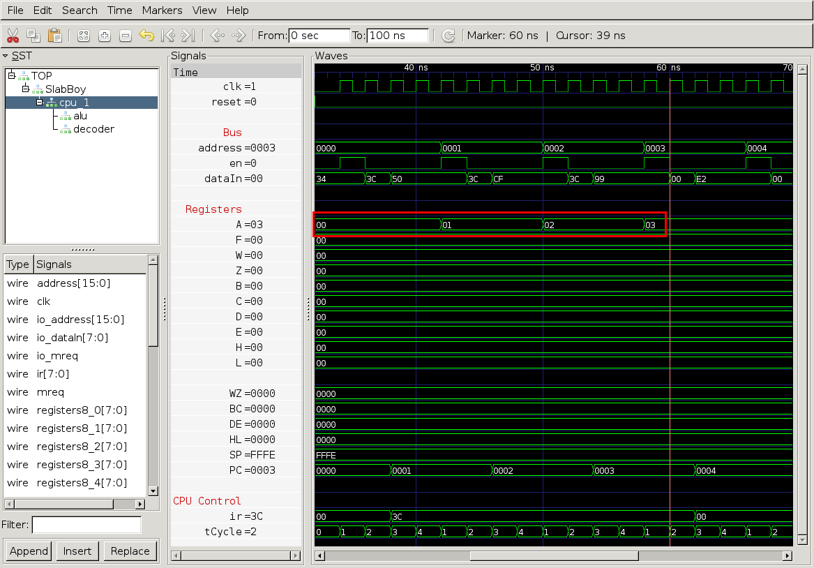 The first instruction works!
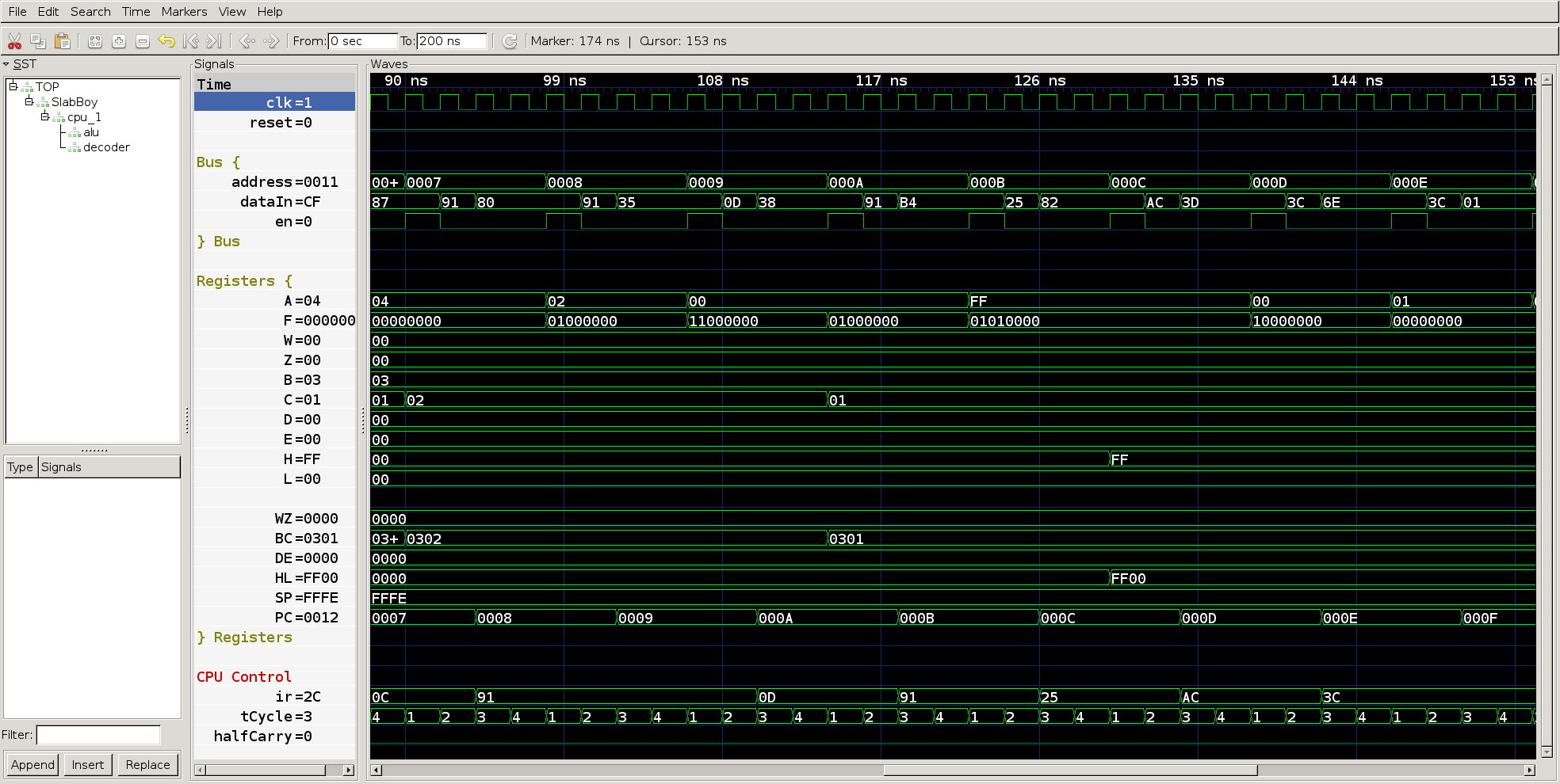
Since it’s so easy to add to the microcode, I’m going to go ahead and put all the 8-bit register-to-register arithmetic instructions into the microcode and add some instructions to test.asm. The microcode is a bit long, so I’ll just link to it here. The new test.asm and resulting waveform are below.
SECTION "ROM0", ROM0

inc a

inc b
inc b
inc b

add a, b

inc c
inc c

sub a, c
sub a, c

dec c
sub a, c

dec h
xor a, h

inc a
inc a
inc a
inc a

inc l

or a, l
Sweet! Next post, we’ll look at implementing memory reads, which are necessary for load instructions and indirect arithmetic instructions.