
FPGA Game Boy Part 1: SpinalHDL and Z80-ish T-Cycles
For a long time now, I’ve wanted to build some hardware emulators of older game consoles on an FPGA. In fact, that was one of the reasons I started designing a handheld game console, the Gameslab, based on the Xilinx Zynq FPGA+ARM combo. Eventually, I envision the Gameslab ARM CPU running an OS that allows you to pick a game, and each game can include custom hardware that is also loaded with the software. For example, one game could run on the ARM CPUs and include some custom graphics hardware on the FPGA fabric for fast rendering of terrain. Or, like the case I want to work on today, the game could load a whole game system into the FPGA fabric. Of course, there will be some trickery involved, and I’ve already started poking around some things, like Linux device tree overlays. However, today I want to start working on something more fun, a HW Game Boy emulator in the FPGA fabric, called the SlabBoy :)
SpinalHDL
So, normally when starting up again on an FPGA hobby project like this, I start to get a little worried the moment I fire up VIM and see some Verilog. Years ago in school, and for a bunch of hobby projects since then, I’ve used Verilog for FPGA projects, and sometimes a little VHDL for working with pre-created IP blocks. However, I’ve noticed a pattern now: I start a new FPGA project with a lot of energy and ideas, and then I slowly lose passion as the dread of Verilog’s verbosity, lack of expressiveness, and dearth of abstractions eat away at my will to live determination. Seriously, Verilog requires a ton of boilerplate just to wire up simple connections, like say an AXI4 bus with a couple dozen signals, let alone attaching a memory-mapped peripheral. Also, Verilog has all kinds of unnecessary foot-guns, like the infamous = vs. <=. At this point, someone might say “why not VHDL then, if you hate Verilog so much?”… I guess the best way to put it is: do you want foot-guns + verbosity - abstractions in Verilog, or verbosity + verbosity - abstractions in VHDL? Luckily, a bunch of smart people in the open-source community have decided this is a worthwhile problem to tackle, and now we have some alternatives to Verilog and VHDL.
Since I’m comfortable with Python, I gravitated first to MyHDL. I won’t go into detail here (the creator of SpinalHDL has a great critique here), but I wasn’t super happy with it. MyHDL drastically improved the syntax for an HDL, removed a bunch of boilerplate, but didn’t get rid of many foot-guns. For example, the weak type system allows you to assign different types and attempts automatic conversion for you. You can even assign different width signals, and it will silently resize them. These are not things I want to happen without knowing, since they are more often bugs than not.
I also tried out another language called Chisel, which is a DSL in Scala from UC Berkeley that spits out Verilog that you can feed into standard synthesis and simulation tools. Though, I didn’t get far into Chisel before I discovered SpinalHDL. Funny enough, I found it while reading critiques of Chisel, in particular the SpinalHDL’s creator’s critique here. Since then, I’ve started to really like SpinalHDL. I have one published repo with some of my early SpinalHDL work: Gameslab LCD controller. That comes from my first few days of SpinalHDL, so I wouldn’t use it as an example of idiomatic code. Instead, I would look at the wonderful SpinalHDL libraries (the built-in standard library).
In fact, the built-in libraries are one of the top reasons I now love SpinalHDL. Implementing a memory-mapped peripheral? Easy; it’s in the libraries and super simple to use: example of APB3 peripheral. Using AXI4 or AXI4-lite? It’s there. 32-bit RISC-V RV32IM CPU? Also there.
What’s a T-Cycle?
It’s a cycle within a machine cycle of the Z80 CPU, or the specialized variant for the Game Boy, the Sharp LR35902. Yup, I’ve been reading way too much about the Z80. Let me back up a minute….
Building the SlabBoy will require writing a few major RTL blocks:
- LR35902-compatible CPU, with hopefully cycle-accurate timing
- Video controller compatible with the Game Boy
- Converter from 160x144 at 2 bits per pixel to the Gameslab’s 800x480 at 24 bits per pixel
- Maybe the sound system, but I still haven’t worked on sound for the Gameslab anyway
Naturally, the CPU is the place to start, since testing everything else will require a CPU compatible with the LR35902. After doing some research, I found a couple of architecture diagrams that help a bit. However, since the Game Boy hardware was full custom, no one really knows what’s inside. So, these diagrams needed a bit of editing.
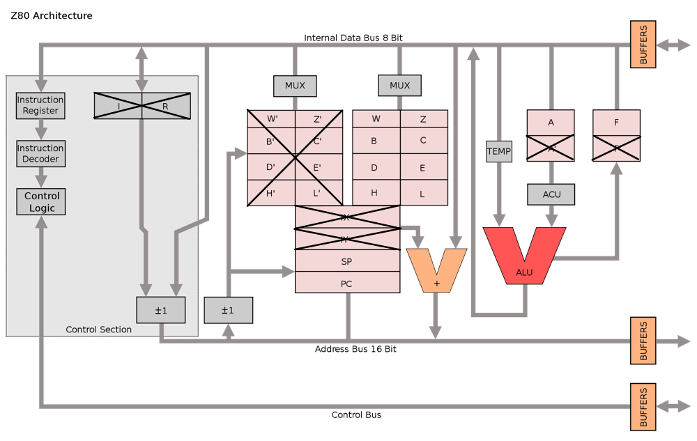 From Spencer Steers's Game Boy Development Book, with some edits.
The are a few immediately noticeable differences from the Z80. First, the LR35902 doesn’t have the additional shadow registers or the IX and IY that the Z80 added to the Intel 8080. Since the Game Boy didn’t use DRAM, so the refresh register is gone, and I can’t find any references to the interrupt vector register. I haven’t looked in detail yet, but it looks like the Game Boy has its own interrupt system. Finally, the last big difference is the unified address space, so IO is memory-mapped in the same space as the RAM. An exhaustive list is here.
To properly run Game Boy ROMs, the SlabBoy will have to implement all the LR35902’s instructions. I found a handy reference site with all the instructions listed with their assembly mnemonics, op-codes, and timing. I’ll use this site’s chart as a checklist while implementing instructions.
It’s also handy to have at least a general idea of the internal timing for the LR35902. From reading the Z80 CPU manual, I learned all about T-cycles and M-cycles. Basically, each M-Cycle performs an operation, a memory read, or a memory write. Each M-Cycle is made up of at least 4 T-Cycles, wherein things like the memory enables, control signals and such are toggled. Combining that knowledge with the diagram below from online, the timing is roughly evident. There will definitely be all kinds of oddities to discover along the way.
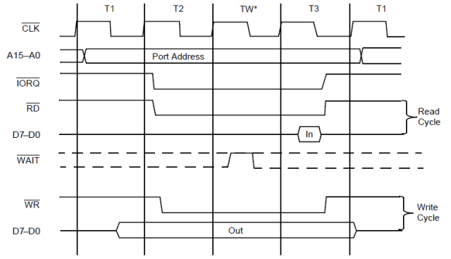 See the T1, T2... at the top, those are T-Cycles
Well, that’s a good start for now. In the next post I’ll go through setting up the SpinalHDL project and getting some of the first CPU instructions implemented.