
SoundSlab: How it Started
“But what if every button is also a screen?” That’s the question that started a multi-year project to build a custom electronic music production device, the SoundSlab. One glorious day it will be part sequencer, part sampler, part synthesizer, and part slab. Today it’s a never-ending hobby project. Here I’ll show you how that project started with impulse buying, a CNC milled PCB, self-inflicted PCB assembly pain, mechanical CAD, 3D printing, and some FPGA fun.
The idea
It all started over beers with buddies, as good projects do. I have a couple best friends that are much more musically inclined than me, and since I was a kid, they’ve always inspired me to get creative and try different instruments. Or in this case, try electronic synthesis gear. This led to a serious, but thankfully short-lived, infection with gear acquisition syndrome (aka GAS). As an avid electronics hobbyist, I think I must be predisposed to GAS (there might be a new microscope on my desk). Anyway, one of my favorite pieces of gear, the Synthstrom Deluge, inspired this project.
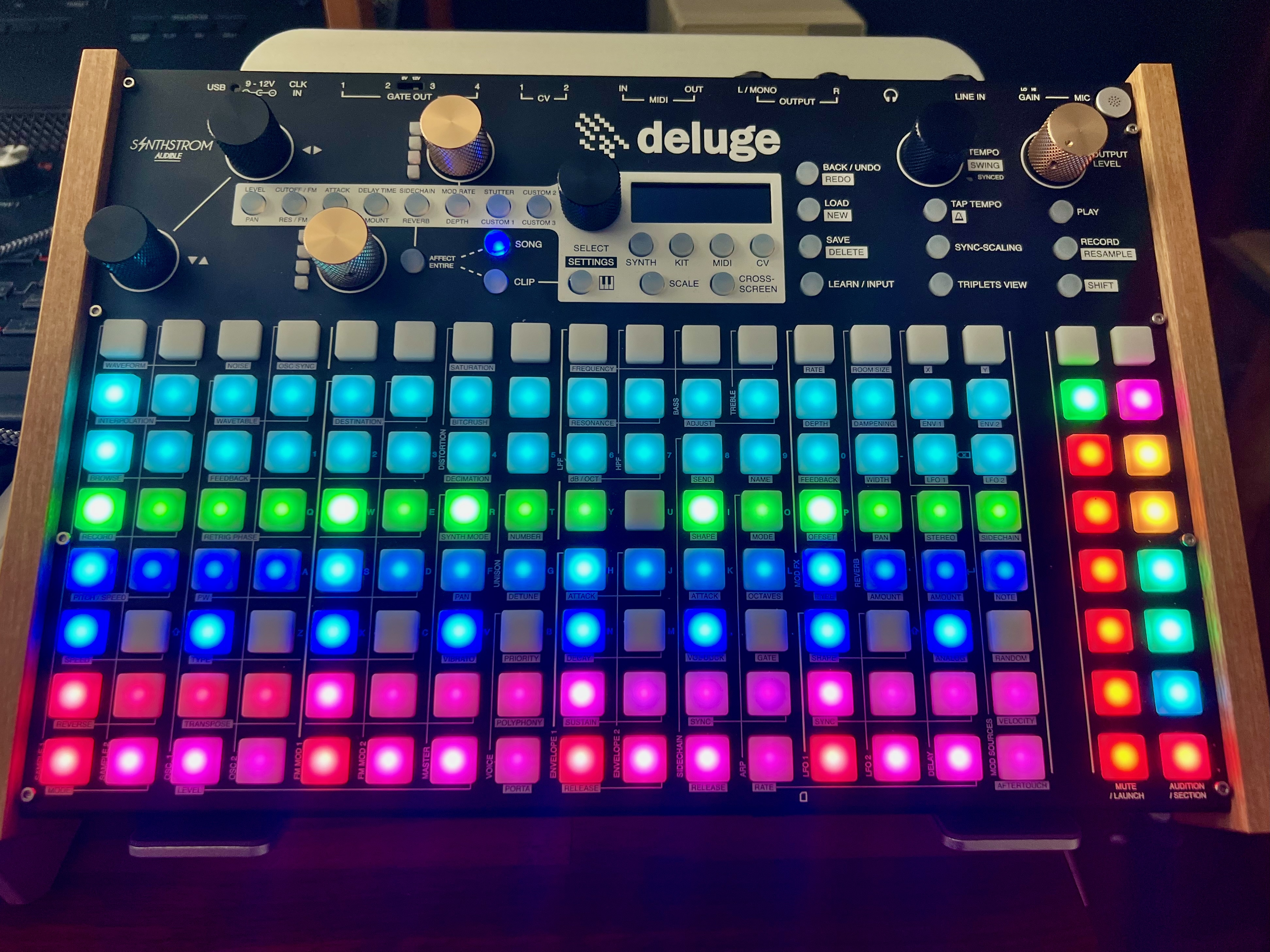 Synthstrom Deluge with 16x8 grid of RGB buttons for sequencing (and other things) with two columns of mute and audition buttons; really fun piece of gear!
The Synthstrom Deluge is a wonderful music production suite in a small box. Its grid of RGB-lit buttons makes sequencing a dream since you get direct visual feedback on eight tracks across the 16-button-wide grid. It also does all kinds of other things, like sampling, waveform editing, synthesis, etc. I won’t go on and on about it. As much as I love it, there are two major issues in my opinion. After you’ve been away from it for a while, the sheer density of functions on a minimal interface make remembering how to do things somewhat challenging. Also, since it just has a tiny screen and RGB LED buttons, there can still be a lot of menu diving. Accessing top level functions is quick, since every RGB button has a secondary function when you hold shift. However, once you’re in a menu, e.g. picking a sample, you’re back to menu scrolling.
“But what if every button is also a screen?” That might change things!
Impulse buying, in bulk
I peruse eBay and AliExpress quite a lot. As a hobbyist hardware hacker, you can get some amazing things that you won’t find anywhere else, like second-hand big FPGA boards, even bigger FPGAs on “cut PCB” instead of cut tape, or a really nice high-end oscilloscope.
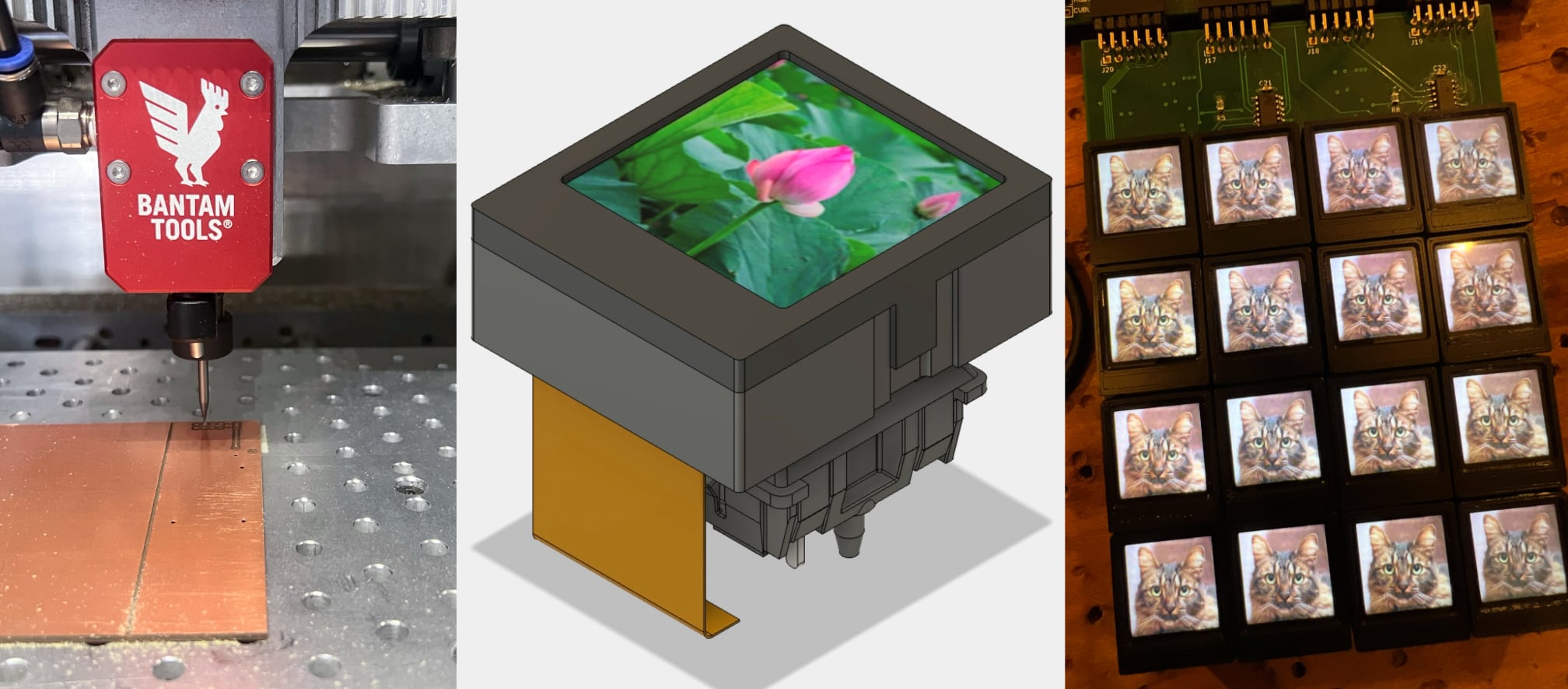
It turns out that on AliExpress, you can find lots of tiny LCD and OLED displays in all kinds of form-factors. Just search “small LCD” or “small OLED”, and you’ll have endless pages of poorly categorized products to flip through. I found some interesting 0.85” 128x128 color LCDs capable of up to 24-bit color. That’s quite sharp! Many sellers offer the same LCD for a few bucks a piece, but one seller was willing to sell them to me for less than $1.80 each if I bought a large quantity. Well, if I was going to build a prototype, I’d need at least 144. And, I usually buy parts for three prototypes, so that’s more than 400 already. So, next thing you know, hundreds of LCDs were on the way. Project started!
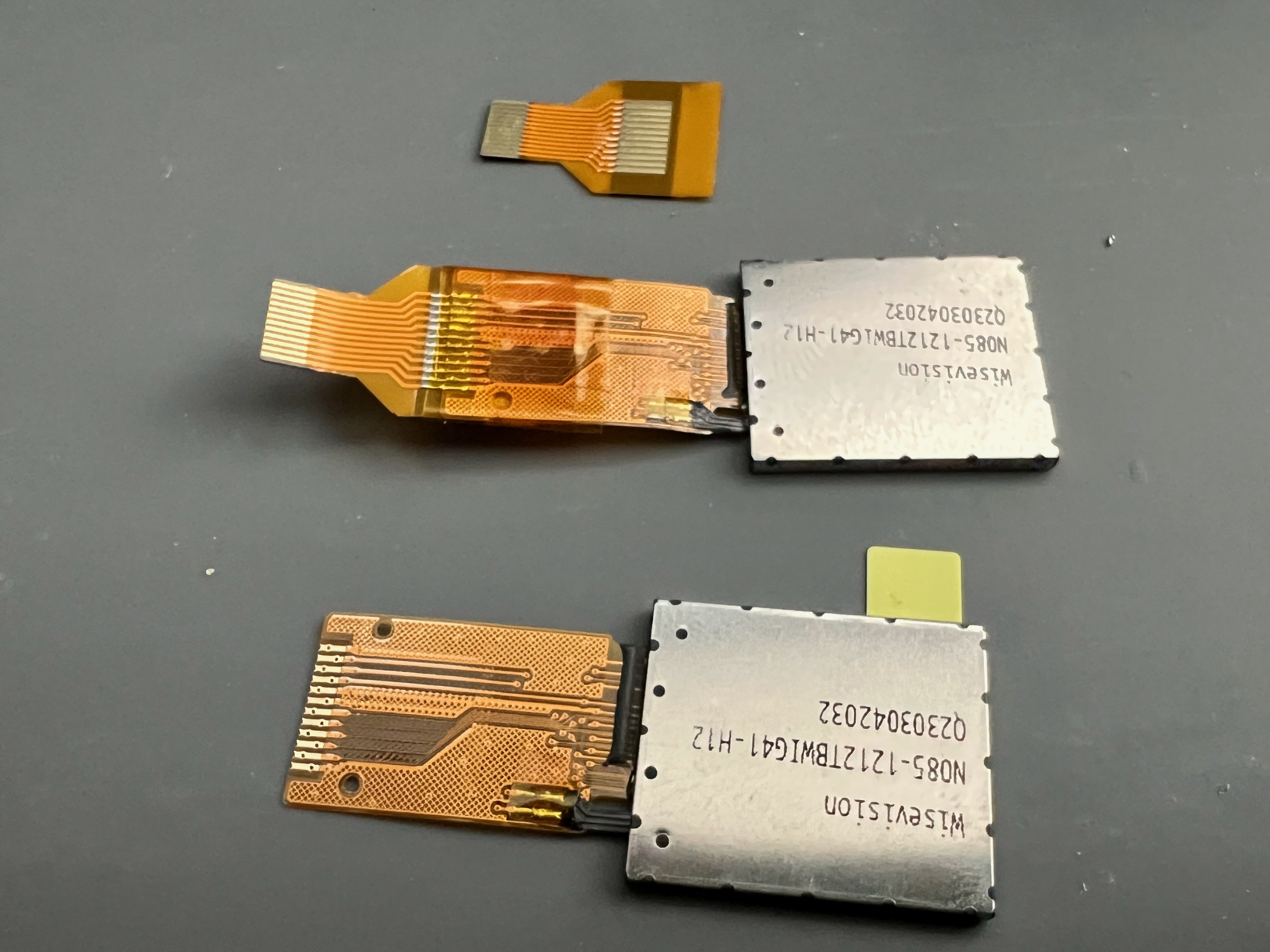
LCD part number: N085-1212TBWIG41-H12 (link to datasheet).
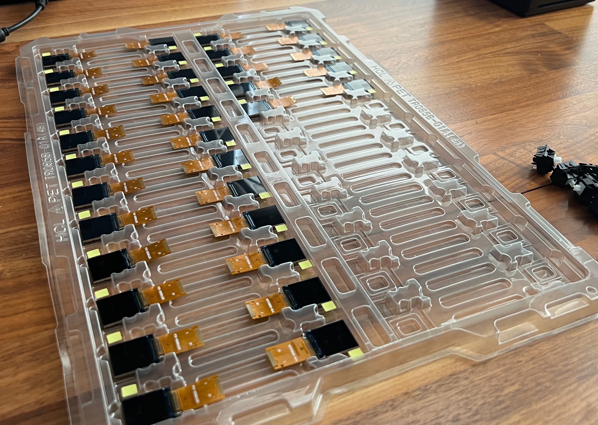
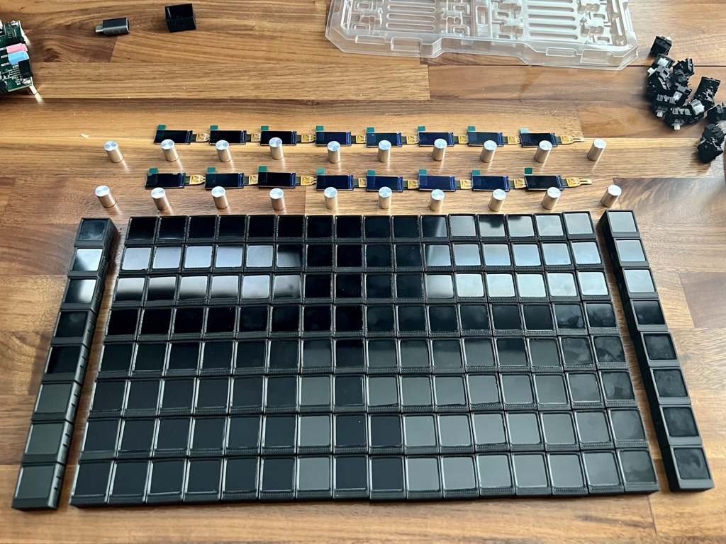
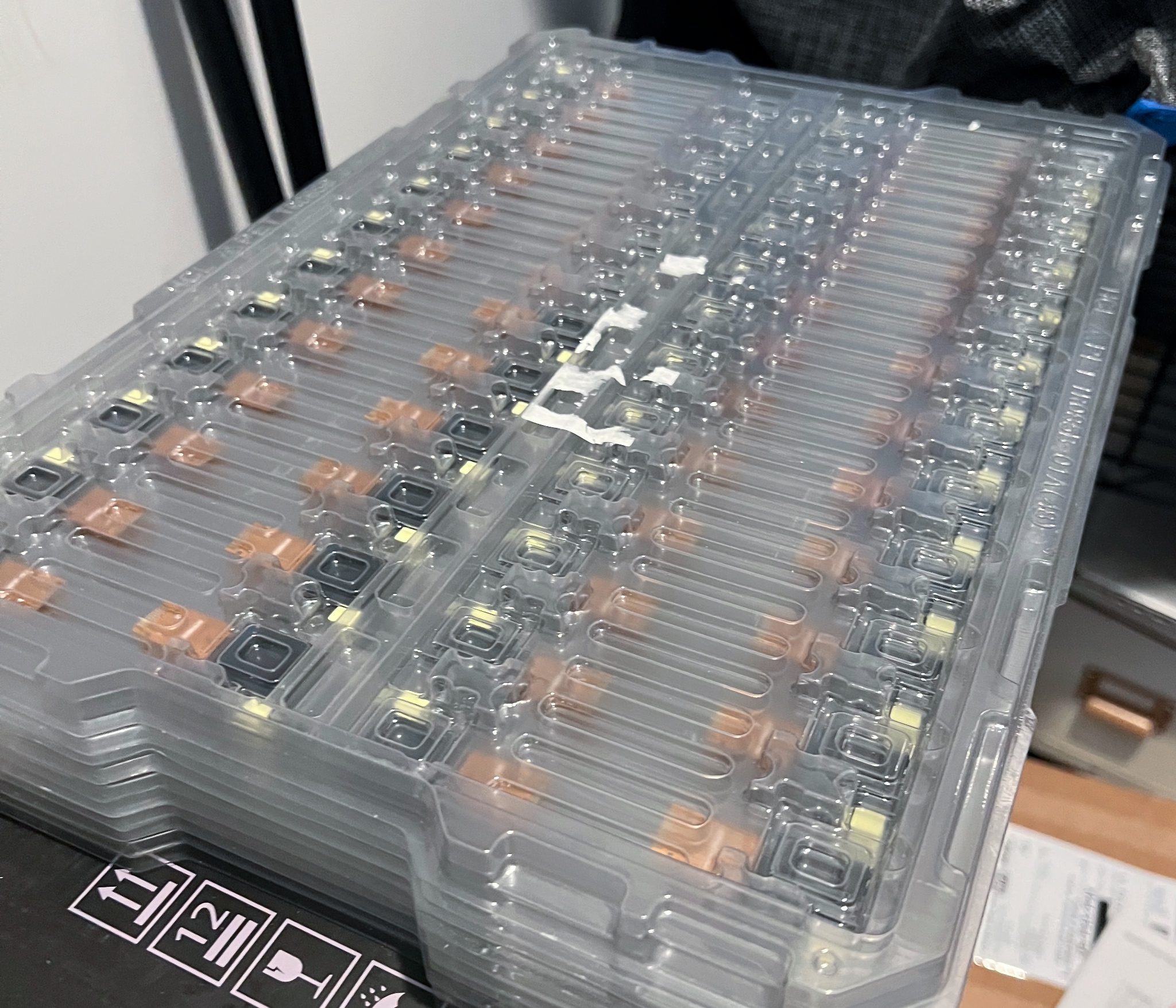 0.85" 128x128 LCDs in plastic trays—all 450 of them!
Taking the LCDs for a spin
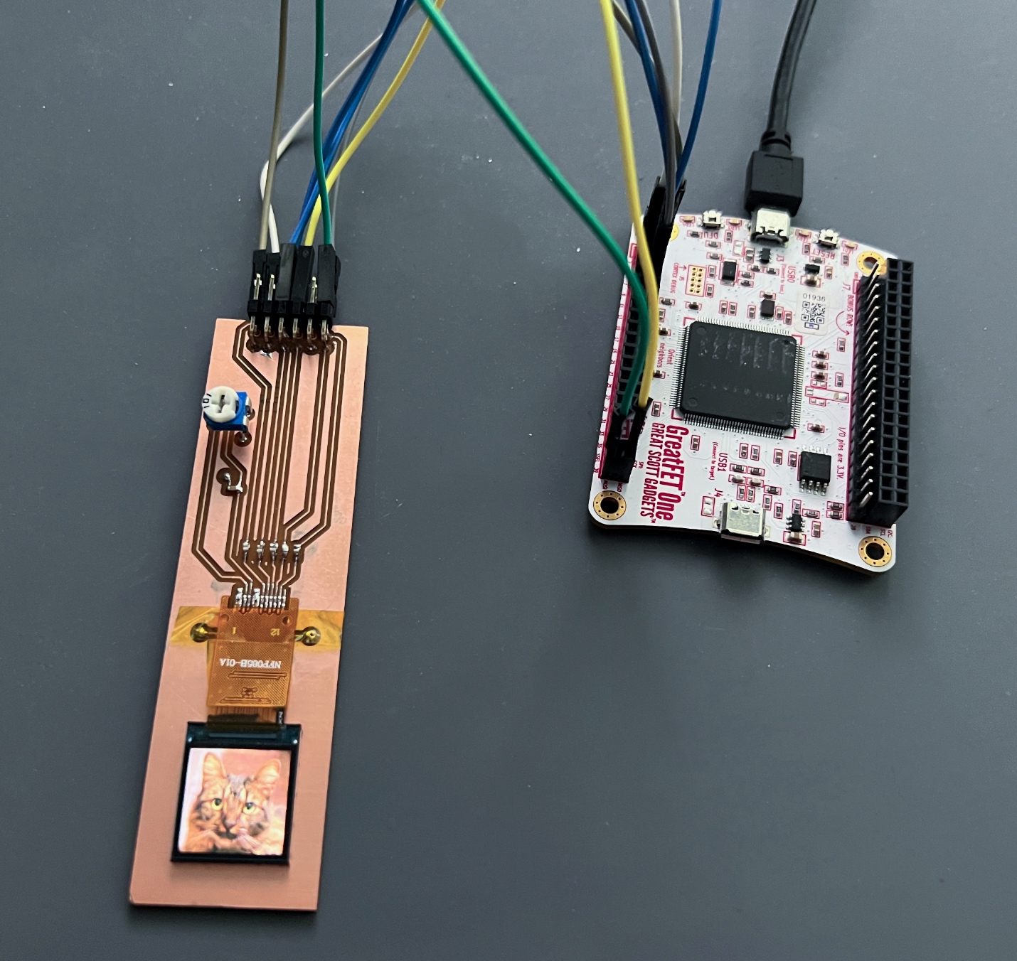
When the displays arrived, I wanted to take them for a test drive and see how fast I could refresh them. Also, there are multiple conflicting initialization routines for these displays out there, so that’d take some figuring out too. There was one little problem though: these displays have 0.7 mm pitch flat-flex cables. It turns out that 0.7 mm pitch is not standard at all and I couldn’t find any off-the-shelf connectors for these. I looked into having a connector manufacturer on Alibaba make some custom ones, and the NRE was much lower than I thought! Thankfully, cooler thoughts prevailed, and I decided to solder the FFC for testing instead of ordering thousands of custom connectors. I’d need a PCB though.
In my garage, I have a desktop CNC (Bantam) that I’ve used for all kinds of projects in brass and aluminum, but I had not tried out PCB milling. This was the perfect opportunity, since I just needed a small adapter board with a really simple pattern. So, I designed a quick PMOD to 12-pin LCD adapter board in KiCad, using through-hole pins of components wherever possible to avoid vias. Any via requires pushing a wire through the hole and soldering both sides since I don’t have an electroless plating setup. Some people use little rivets made for this purpose, but I found some wire works just fine for a few vias.
On the CNC, I fixtured up a copper-clad FR-1 blank that I’d ordered years ago, anticipating this moment. When you CNC mill PCBs, it’s important to use something like FR-1, not standard fiberglass FR-4. CNC milling produces lots of dust, and you don’t want to breathe in FR-4 dust! For holding a flat workpiece like a PCB in place, I’m partial to double-sided Nitto tape. If that’s a bit pricy, painters tape on each side with super glue between also works. I’ve done that a few times on taller parts where I was more worried about chatter. After an hour or so of setup and milling, I think the PCB came out pretty nicely.
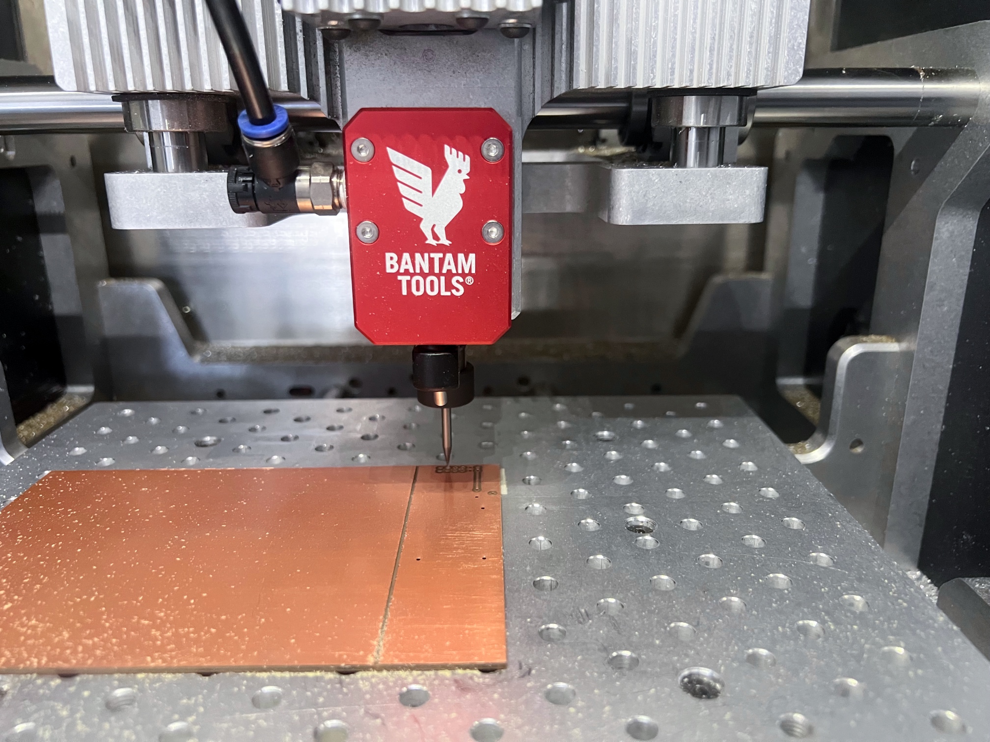 The compressed air cooling wasn't really necessary for this milling job, but it kept dust out of the way so I could see the action
 Those little blobs on each trace are surface-mount test points that I tried out. They didn't work so well here.
To get the LCD going quickly, I pulled out one of the many “utility knife” boards that I have laying around—a GreatFET One. The Python API for it is pretty nice, and it supports running the SPI peripheral at decently high speed. The firmware and host Python code do some fancy buffering to make it fast. Once I figured out the initialization routine, I was able to drive these LCDs at up to 90 MHz!
Initialization routine in Python for the GreatFET One
That high speed is necessary. I wanted a grid of at least 18x8 LCD buttons refreshing at 60 Hz for butter smooth animations. Yes, totally necessary. Looking at the data rate calculations:
| Resolution | Bits Per Pixel | Refresh Rate | Data Rate | Data Rate for 4 LCDs |
|---|---|---|---|---|
| 128x128 | 24 | 60 Hz | 23.6 Mbit/s | 94.4 Mbit/s |
| 128x128 | 24 | 30 Hz | 11.8 Mbit/s | 47.2 Mbit/s |
| 128x128 | 16 | 60 Hz | 15.7 Mbit/s | 62.9 Mbit/s |
| 128x128 | 16 | 30 Hz | 7.9 Mbit/s | 31.4 Mbit/s |
The SPI data-rate would directly determine how many LCDs I could drive with a single SPI bus. 24-bit color was tempting, but I found 16-bit color was just fine for most cases on these LCDs. It doesn’t seem like these small LCDs really respond accurately to the lower bits anyway. So, with 16-bit color at 60 Hz and in groups of four LCDs per bus, I’d have to run at > 63 MHz. Since my testing showed that they work even up to > 90 MHz, that seemed reasonable with some safety margin for part-to-part tolerances. For the full-size grid, that’s still a lot of SPI buses! 144 LCD buttons would require 36 SPI buses running at > 63 MHz!
I don’t know of any microcontrollers that come with 36 SPI peripherals and a HDMI input. I’m kind of an FPGA guy, and I knew that even a lower-end Xilinx Artix 7 with GTP transceivers could sink HDMI and output 36 SPI buses at 63 MHz without breaking a sweat. The test PCB has a PMOD connector on it, and that fits perfectly into a Digilent Zybo dev board on my desk. With a little bit of SpinalHDL gateware, I was able to drive the LCD reliably. Time to go bigger.
 It turns out that outputting a clock from an FPGA should be done with care. You don't just run a clock to an IOB. You put something like an ODDR with data set to alternating 1s and 0s
What about the button part?
With the LCDs working, it was time to turn them into buttons. I’d considered all kinds of tactile switches, domes, and even DIY pressure sensitive pads made with velostat. However, my decision was cast one day while playing with another piece of gear, my Elektron Digitakt. It has a bunch of buttons on it that have incredible clicky action. They feel just like Cherry MX mechanical keys. Hmmmm… that idea stuck. Why not use mechanical key switches? They come in all different variants, clicky to quiet, and they have a stem for easily mounting a key cap. I’d just need a key cap that holds a LCD in place, and I bet I could make that.
Initially, I thought of a little two-piece key cap held together by some tiny screws. After considering how tedious that would make assembly, I landed on a design with snap tabs on each side. Assembly would just require putting the LCD inside and snapping together—much easier. I had been learning to use Fusion 360 for a few years on-and-off since its built-in CAM was great for my CNC mill. So, I modeled the LCD key cap and checked how it looked against a Cherry MX switch model I found online.
 I've done a few revisions to the design since this one, but the basic form is still the same
My first attempt at making these was a bit insane. I had the crazy idea that I’d mill these out of aluminum. Just like you’d guess, that was a bad idea. These parts have really thin floors and sidewalls, which requires great repeatability for fixturing. Also, the snap tabs have to bend without deforming. Thin aluminum isn’t so great for that. So, let’s just forget about that misadventure.
3D printing is definitely the better way to go for these key caps. I can print them in batches of 16 in PLA, PETG, or ASA. Unlike aluminum, plastics work well for making snap fit tabs that don’t break off or deform. PLA and ASA produced caps with the nicest finish and overall look. The PETG ones in the pictures are too shiny around the LCD screens.
The 3MF file for the LCD key cap is available here.
 This PETG is a bit too shiny. In later revisions, I also use non-uniform layer heights to improve the bevel around the screen.
 It was easy to get a little carried away and print all of them...
Flat flex fix
Remember how the LCD flat flex cable (FFC) had a non-standard 0.7 mm pitch that I couldn’t find any connectors for? Well, it also turns out that when they’re mounted in a key cap on top of a mechanical key switch, they were too short! The FFCs were just long enough to make it to the PCB, but there wasn’t any room for a bend or connection. Thoughts about custom connectors surfaced again. Friends at Hardware Happy Hour suggested vertical riser PCBs. Finally, I decided I’d just make extension cables. If I could solder a FFC extender onto each LCD’s cable, I could also convert the 0.7 mm pitch to a standard 0.5 mm pitch with many connectors readily available in all styles. That would also make it much easier to switch out LCDs if any of them died (foreshadowing).
So, I did just that. I fabbed a big bag of FFC extenders at JLCPCB and soldered a bunch of them onto LCD cables. You might think soldering these sounds like a pain in the butt, but the trick is flux! With a little practice to get the right amount of solder, you just wipe all the pads with a flux pen, then drag the iron back-and-forth across all the pads. In a few seconds, all the pads are soldered without shorts. I also added a little bit of Kapton tape to keep stress off the solder joints, but I’m not sure that will hold over time.
KiCad and Gerber files for the latest revision are available here.
 Each FFC extender also has a stiffener below the solder area to prevent stressing the joints. Since this, I've done a revision to extend the length further and wrap over the bottom of the key for a better connection angle.
Scaling up
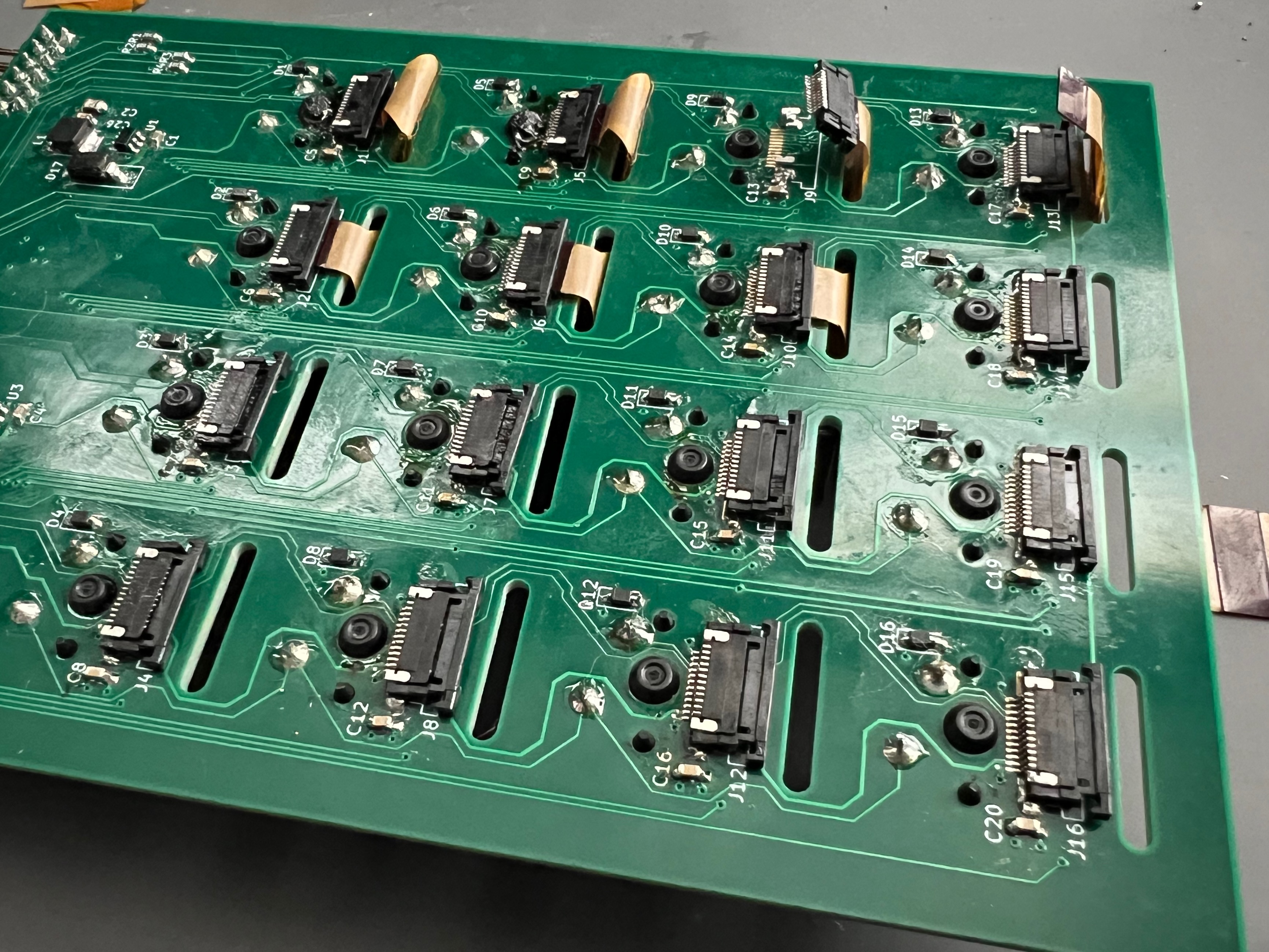
Before ordering the big expensive full-size grid, I wanted to build a smaller prototype: a 4x4 grid. This prototype would critically test driving the LCDs in clusters of four per SPI bus and how well the FFC extenders survive when a switch is actuated many times. The datasheet for the LCDs says 3.0 V nominal, 3.1 V max on the backlight LEDs, so I could chain together eight of them and be at 24.8 V worst-case. That’s within the voltage range for common LED backlight drivers, like the AP3032 in this design. The design also used a 74xx139 de-mux on the chip select lines for each cluster of four LCDs. That helped fit within the available pins on the PMOD connectors (and I’d use that same strategy in the full-scale design later).
 KiCad schematic in the nice Gruvbox color scheme
 I've caught many design mistakes before using 3D renders in KiCad
You know when you tell yourself that you’re not going to do that again, then 6 months later you do it again and regret it… again. Well for the ButtonSlab prototypes, I ordered PCBs and thought “that’s not too many parts, I’ll go without a stencil and just solder by hand”. What a mistake! I have a nice toaster oven reflow controller, and I still for some reason thought I’d do these without paste.
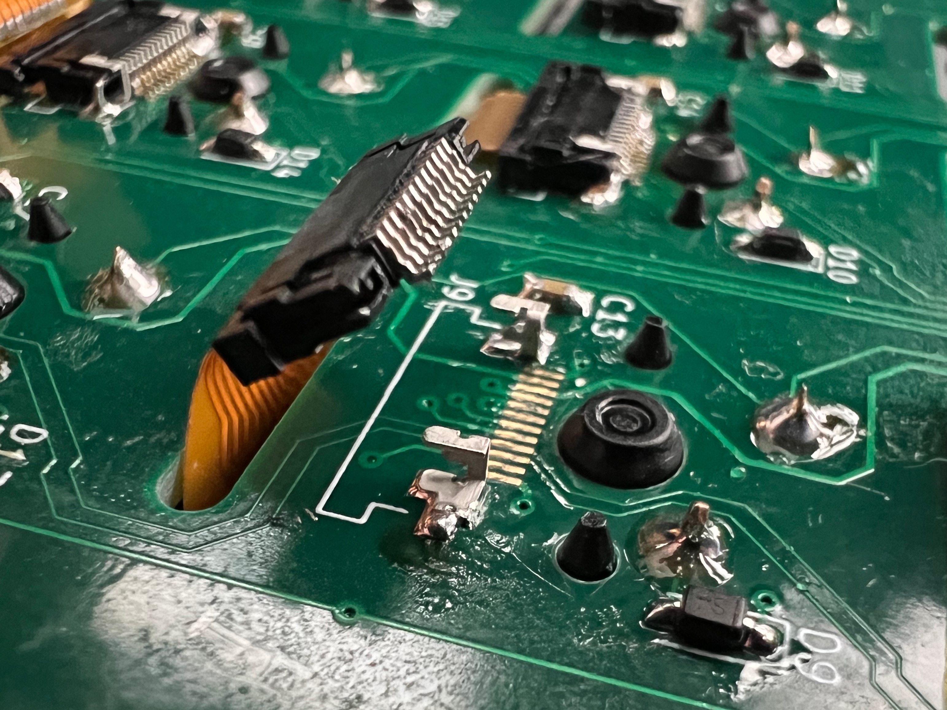
All 16 LCD key footprints have a surface-mount FFC connector, and those have gull wing leads. For some reason, these connectors were particularly hard for solder to wet and wick around, even drenched in flux. Eventually, I did get all the connectors soldered without shorts. Do yourself a favor, always order the stencil and use solder paste with reflow for gull wing leads. Stencils and paste are so cheap and will save so much time.
 Just order a solder paste stencil and do reflow. It will prevent so much frustration!
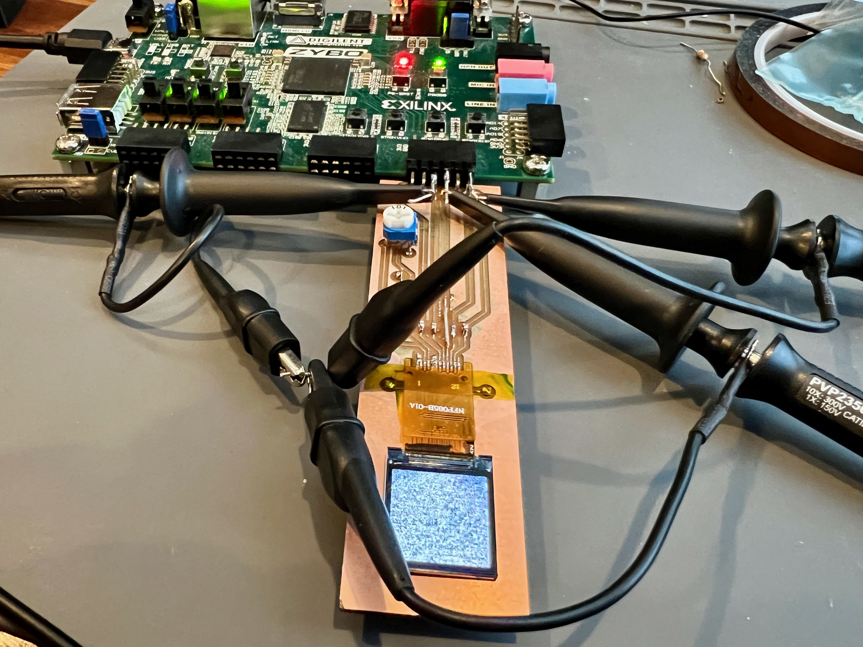
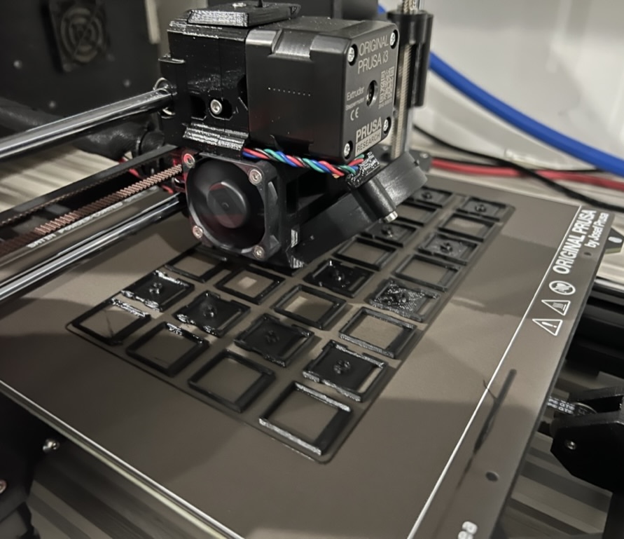
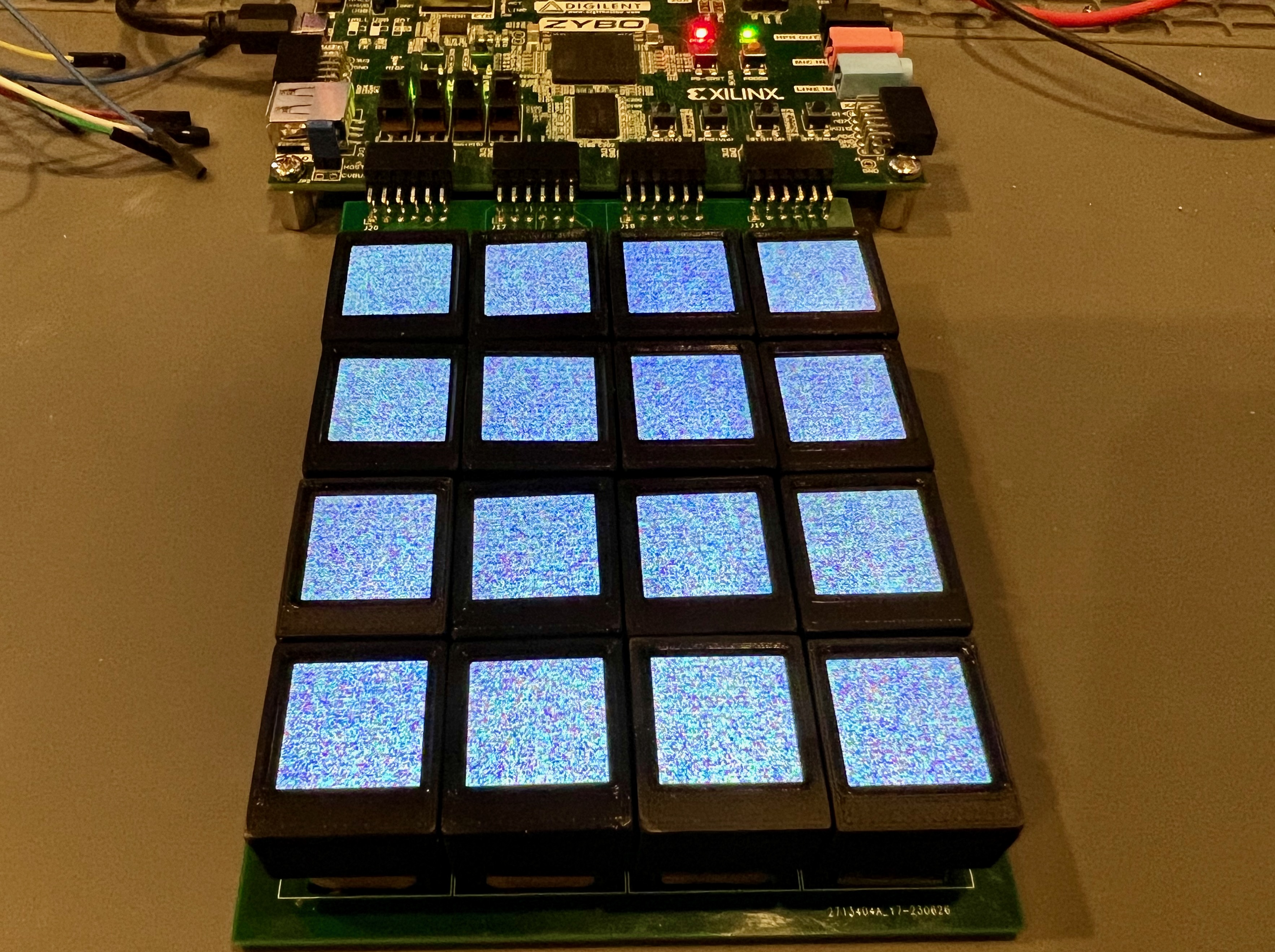
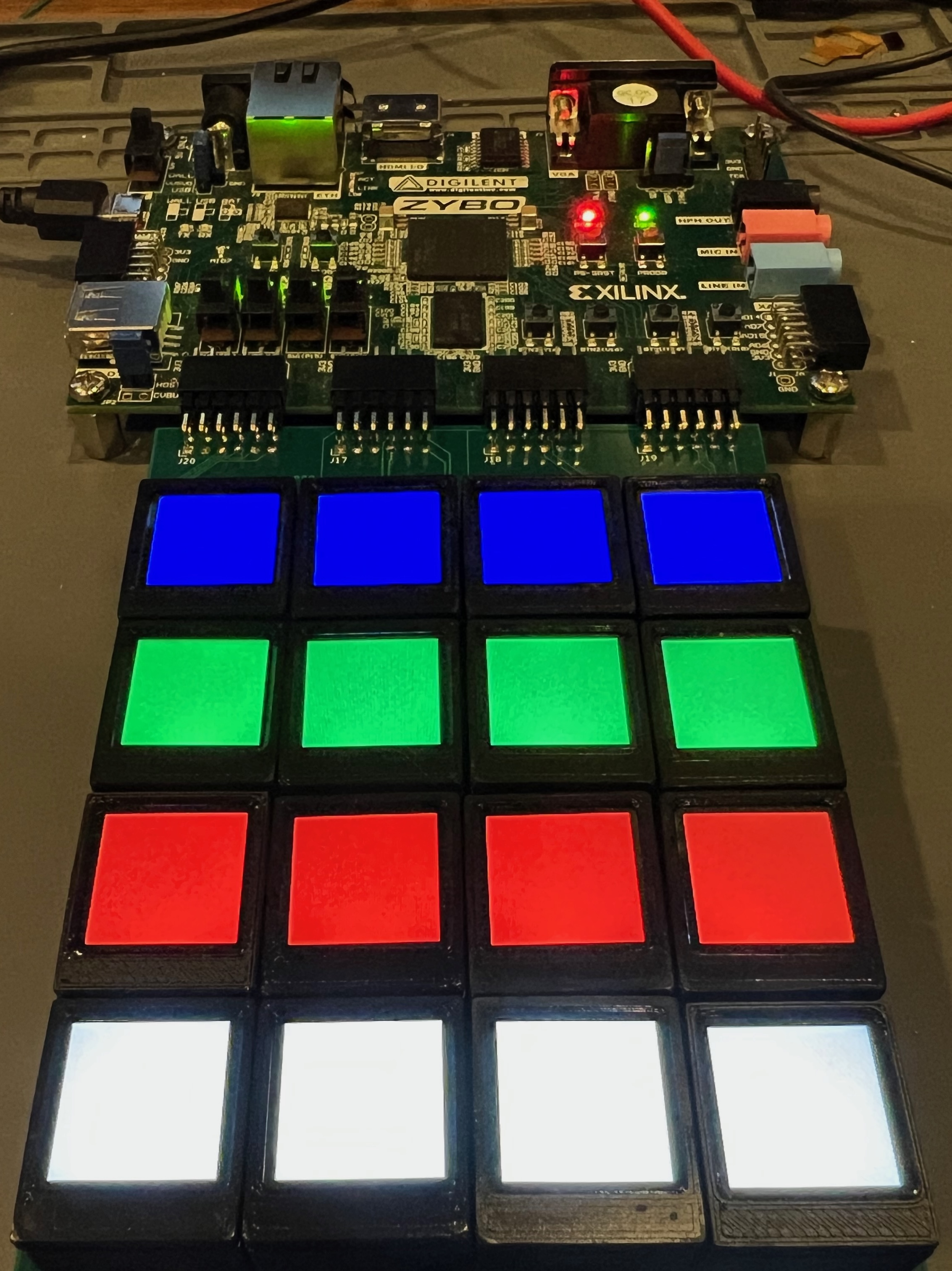
Once assembled, I tested a single column using the GreatFET One since I already had working code. This minimized variables since the backlight driver and cluster connectivity were already different. I had to change the initialization to flip the picture around (the LCD was in the other orientation on the test board), but it worked other than that. So, I quickly moved to putting together some SpinalHDL gateware to drive the full 4x4 grid. It may not look too exciting, but that 4x4 grid of random pixels, “snow”, was so satisfying. That meant the initialization routine had been successful for all 16 LCDs. I was able to get images onto the LCDs pretty quickly after that.
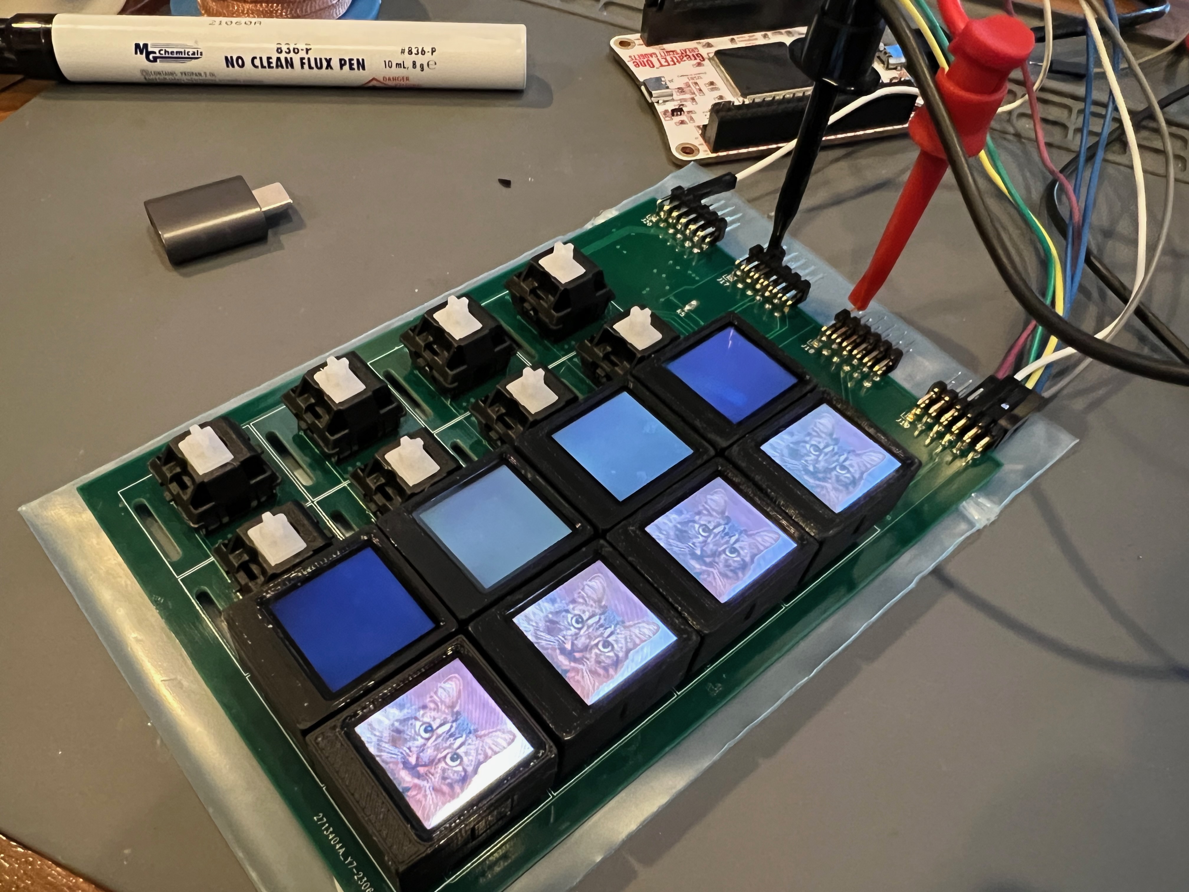
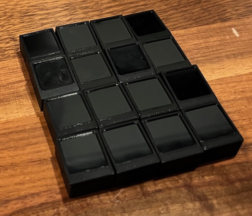
 That's Benedict, our cat, on the left. His picture shows up a lot on the SoundSlab. On the right, that's what we call "snow" (namesake of the Stephenson novel, Snow Crash). When the LCDs start up, the framebuffer RAM contains random data, so that's what you see on the screen.
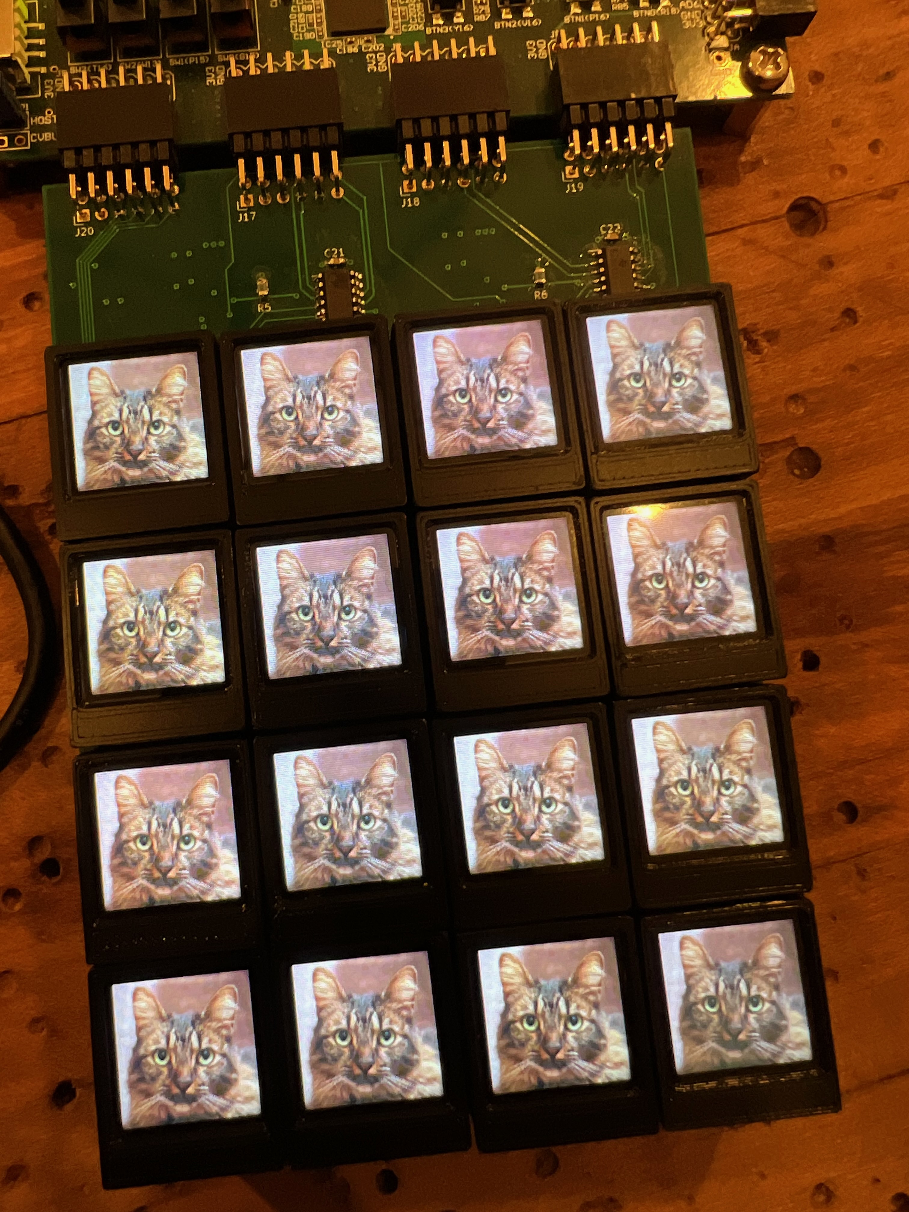 That's our cat Benedict again. He looks pretty good in 16-bit color.
Signal integrity matters, I guess
When I eventually started testing video at 60 Hz, not just static images. I noticed a problem: flickering. Specifically, only some lines of some LCDs were flickering, sometimes. That’s what I call a heisenbug. Or in this case, poor signal integrity. I put a scope on the SPI lines, and the problem was pretty obvious. The signal edges look like crap with the increased capacitive load of four LCDs, connectors, and FFC extenders. That’s why 90 MHz worked just fine on a single LCD, but this issue popped up on the larger array.
WARNING: flashing lights
That would be a cool effect for a demoscene project. If only signal integrity issues were deterministically controllable like that…
Luckily, a friend at Hardware Happy Hour reminded me that Xilinx FPGAs have controllable IO drive strength. This probably created an EMI nightmare, but it did solve my signal integrity problem. In the later full-scale design, I incorporated buffers to redrive the SPI buses on the grid PCB.
set_property -dict { \
    PACKAGE_PIN AD17 \
    IOSTANDARD LVCMOS33 \
    DRIVE 16 \
} [get_ports { SCL[0] }];
...
What’s next?
This post is years late. In fact, I think all of this was done in 2023, so I’m over two years late posting it. I’ve already built a full-scale SoundSlab grid and even a custom FPGA driver board for it with HDMI input. So, in following posts I’ll dive into that. The fun did not end here. Also, I’m working on a cleaned up version of the KiCad footprints for the LCD buttons. Even the 2nd revision used in the full-scale grid had the slots slightly out of place where the FFC rubbed on the PCB edge. I hope to release that as a KiCad library with the footprints and 3D models.
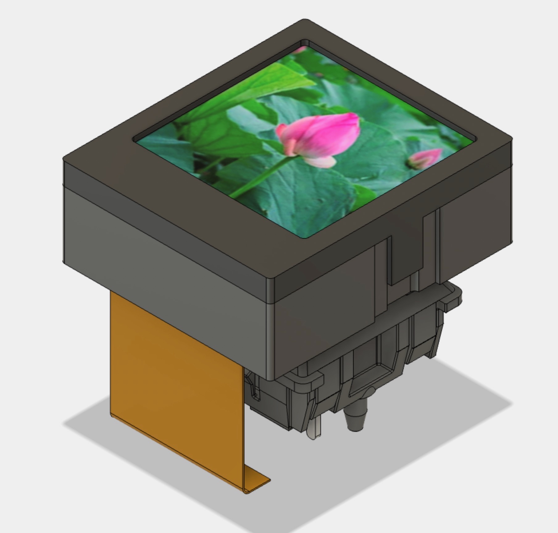
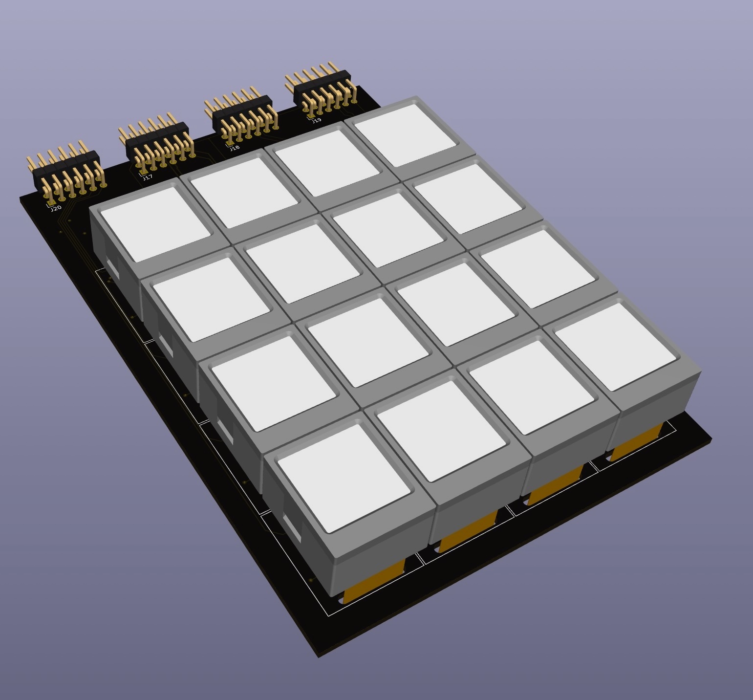
In the meantime, here’s a teaser of what the full-scale SoundSlab looks like: